W25QXXX NOR Flash Chips SPI
Eight pin SPI flash chips are a cheap and easy way to add storage to your project. They’re available in sizes from 1MB to 128MB, and can be used to store data, firmware, or even a filesystem. They’re commonly found on PC motherboards for storing BIOS, FPGAs for storing bitstreams, and even the Bus Pirate for storing the firmware.
Get Bus Pirate & Accessories
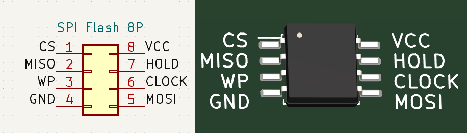
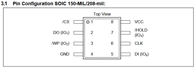
Connections
| Bus Pirate | SPI Flash | Description |
|---|---|---|
| CS/IO5 | CS | Chip select |
| MISO/IO4 | DO | MISO Controller Data In |
| MOSI/IO7 | DI | MOSI Controller Data Out |
| CLK/IO6 | CLK | SPI Clock |
| WP/IO3 | WP | Write Protect, HIGH to disable |
| HOLD/IO2 | HOLD | Hold, HIGH to disable |
| Vout | VCC | 3.3volt power supply |
| GND | GND | Ground |
Connect the Bus Pirate to the SPI flash chip as shown in the table above. Don’t forget the the write protect (WP) and hold pins, or the chip may not behave normally.
SPI Flash Adapters
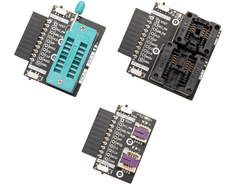
SPI flash adapters for SOP8, WSON8, and DIP8 chips are available for Bus Pirate 5 and up. Connect SPI flash chips to the Bus Pirate quickly and easily.
| Package | Chip | Capacity |
|---|---|---|
| DIP8 | Winbond W25Q80BV | 8Mbit |
| SOP8 | Winbond W25Q80DV | 8Mbit |
| WSON8 | Winbond W25Q64CV | 64Mbit |
Flash adapter boards include a sample chip so you can get started right away. This demo uses the chips included with the adapters. The datasheets are linked above.
See it in action
Setup
HiZ> m spi

Mode: SPI
SPI speed
 1 to 62500kHz
 x. Exit
kHz (100kHz*) > 100
Data bits
 4 to 8 bits
 x. Exit
Bits (8*) > 8
Clock polarity
 1. Idle LOW*
 2. Idle HIGH
 x. Exit
Polarity (1) > 1
Clock phase
 1. LEADING edge*
 2. TRAILING edge
 x. Exit
Phase (1) > 1
Chip select
 1. Active HIGH (CS)
 2. Active LOW (/CS)*
 x. Exit
CS (2) > 2
Actual speed: 99kHz
SPI>
The most common NOR flash chips have an SPI interface. Flash chips are generally capable of 104MHz, but due to the adapter, cable length, breadboard, and other factors, we’ll use a low low speed of 100kHz.
m spi- change to SPI mode, or just hitmto select from the menu.100- set SPI speed to 100kHz.- Hit
enterto select the default values for the other options (8 data bits, idle low, leading edge, CS active low)
Power supply
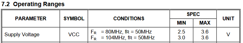
According to the datasheet, the W25QxxxV series of chips can operate at 2.5 to 3.6 volts, with a slightly higher minimum voltage for speeds above 80MHz.
Image source: datasheet
SPI> W 3.3
3.30V requested, closest value: 3.30V
300.0mA requested, closest value: 300.0mA

Power supply:Enabled
Vreg output: 3.3V, Vref/Vout pin: 3.2V, Current: 2.9mA

SPI>
Let’s set the Bus Pirate to power the chip at 3.3volts, a very common voltage for modern SPI devices.
W 3.3- enable the onboard power supply at 3.3 volts.
WP and HOLD pins
Most SPI flash chips have a write protect pin (WP) that prevents accidental writes, and a hold pin (HOLD) that pauses the chip.
- HOLD must be held high or the chip won’t respond.
- WP must be held high or the chip will be read only.
Often the chip will not respond if is WP is left floating, so be sure to hold it high (write enabled) or low (write disabled).
SPI> A 2; A 3
IO2 set to OUTPUT: 1

IO3 set to OUTPUT: 1

SPI>
Set HOLD (IO2) and WP (IO3) high with the auxiliary pin commands.
A 2; A 3- Use Auxiliary pin control to set IO2 and IO3 high
Ensure WP and HOLD pins are held high or the chip may not respond.
Identify the chip
| Device | Manufacturer ID | Device ID | JEDEC ID |
|---|---|---|---|
| W25Q80BV | 0xEF | 0x13 | 0xEF 0x40 0x14 |
| W25Q80DV | 0xEF | 0x13 | 0xEF 0x40 0x14 |
| W25Q64CV | 0xEF | 0x16 | 0xEF 0x40 0x17 |
SPI flash chip commands are loosely standardized on some historical trends, but each manufacturer tends to add their own extensions.
We’ll try to use the most common commands, but not all chips will respond to all commands!
Reset ID
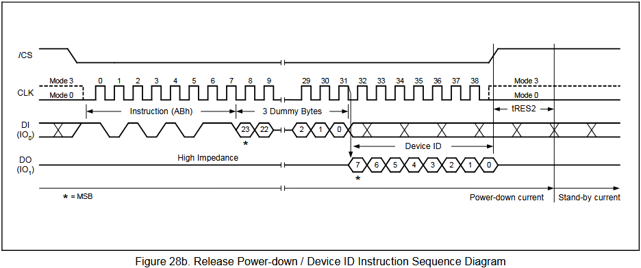
The Reset ID is available immediately after the chip is reset. Write instruction 0xAB and three dummy bytes, then read the one byte reset ID.
- CS pin is pulled low
- Send the instruction
0xAB - Send three dummy bytes
0x00 - Read the reset ID/device ID byte
- CS pin is pulled high
The chip must be reset before reading the reset ID. This is done with the Power Down instruction 0xB9, followed by a delay of 10ms.
SPI> [0xb9] D:10 [0xab 0x00:3 r]

CS Enabled
TX: 0xB9
CS Disabled
Delay: 10ms
CS Enabled
TX: 0xAB 0x00 0x00 0x00
RX: 0x13
CS Disabled
SPI>
Let’s reset the chip and read the reset ID.
[- Start of SPI transaction. Lowers the CS pin to ground.0xb9- Write the Power Down instruction.]- End of SPI transaction. Raises the CS pin to 3.3volts.D:10- Delay 10ms.[- Start of SPI transaction. Lowers the CS pin to ground.0xab- Write the Reset ID instruction.0x00:3- Write three dummy bytes using the repeat command.r- Read a one byte response.]- End of SPI transaction. Raises the CS pin to 3.3volts.
The response 0x13 (or 0x16 for W25Q64) is the reset ID of the flash chip.
Reset ID is primarily a way for a device to determine which flash chip is present among several known options. There’s no standard, and about the only way to find it is by digging through datasheets.
Read Electronic Manufacturer ID
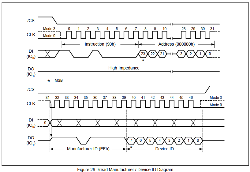
The Read Electronic Manufacturer ID instruction 0x90 returns a one byte manufacturer ID and a one byte device ID.
- CS pin is pulled low
- Write the Read Electronic Manufacturer ID instruction
0x90 - Write the 24 bit (3 byte) address
0x000000 - Read the Manufacturer ID and Device ID bytes
- CS pin is pulled high
SPI> [0x90 0x00:3 r:2]

CS Enabled
TX: 0x90 0x00 0x00 0x00
RX: 0xEF 0x13
CS Disabled
SPI>
The Read Electronic Manufacturer ID does not require a reset, we can issue this command at any time.
[- Start of SPI transaction. Lowers the CS pin to ground.0x90- Write the Read Electronic Manufacturer ID instruction.0x00:3- Write the 24 bit (3 byte) address 0x000000.r:2- Read two bytes of data. The first byte is the manufacturer ID, the second byte is the device ID.]- End of SPI transaction. Raises the CS pin to 3.3volts.
0xEF is the manufacturer ID: Winbond. 0x13 (or 0x16 for W25Q64) is the device ID of the flash chip, same as the Reset ID command.
The manufacturer ID is a unique value assigned to each manufacturer - except they ran out of IDs and started duplicating ages ago so it’s not super useful. JEDEC maintains a list of IDs (free but agreement required) that can help narrow it down somewhat.
Like the Reset ID, the Electronic Manufacturer ID is primarily a way for a device to determine which flash chip is present among several known options. There’s no standard, and about the only way to find it is by digging through datasheets.
Read JEDEC ID
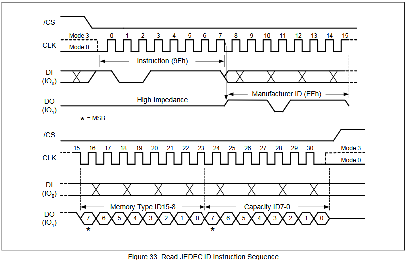
The Read JEDEC ID instruction 0x9F returns a three byte response. The first byte of the response is the Manufacturer ID. Winbond uses the second byte as a memory type ID and the third byte as a capacity ID, but this varies by manufacturer.
- CS pin is pulled low
- Write the Read JEDEC ID instruction
0x9F - Read the manufacturer ID, Memory Type ID and Capacity ID bytes
- CS pin is pulled high
SPI> [0x9F r:3]

CS Enabled
TX: 0x9F
RX: 0xEF 0x40 0x14
CS Disabled
SPI>
Unlike the previous two ID instructions, the Read JEDEC ID command does not require (dummy) address bytes. The instruction is executed and the response is returned immediately.
[- Start of SPI transaction. Lowers the CS pin to ground.0x9F- Write the Read JEDEC ID instruction.r:3- Read three bytes of data. The first byte is the manufacturer ID, the second byte is the memory type ID, and the third byte is the capacity ID.]- End of SPI transaction. Raises the CS pin to 3.3volts.
The manufacturer ID is 0xEF: Winbond. Memory type ID is 0x40, and the capacity ID is 0x14 (or 0x17 for W25Q64).
Manufactures use different systems to encode memory type and capacity ID for each chip. There is no universal standard for these values, and they can vary between manufacturers and even between different chips from the same manufacturer.
Read SFDP tables
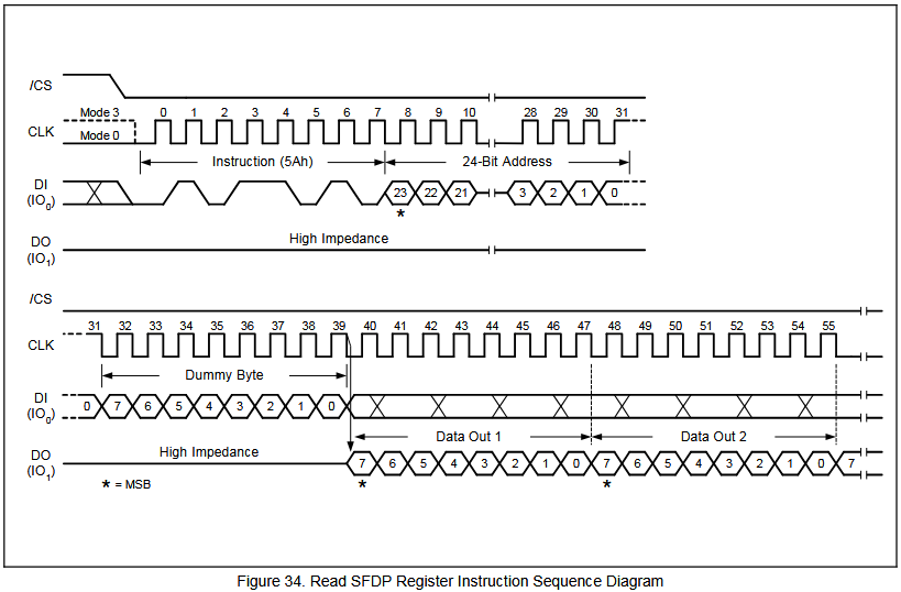
We’ve tried three ID commands that don’t give us a ton of useful information. Eventually flash manufacturers got together and designed a standard system to describe the chip, its specifications and the instructions to access it: Serial Flash Discoverable Parameters (SFDP) tables.
The Read SFDP tables instruction 0x5A returns up to 256 bytes of data.
- CS pin is pulled low
- Write the Read SFDP instruction
0x5A - Write the 3 byte address
0x00000000that indicates where we want to being reading within the 256 byte SFDP table - Write one dummy byte
0x00 - Read the SFDP table header (8 bytes)
- CS pin is pulled high
SFDP tables are not always present, especially in older flash chips (in through hole DIP packages). If the chip does not support SFDP, the response will be 0xFF.
SPI> [0x5A 0x00:3 0x00 r:8]

CS Enabled
TX: 0x5A 0x00 0x00 0x00 0x00
RX: 0x53 0x46 0x44 0x50 0x05 0x01 0x00 0xFF

CS Disabled
SPI>
Send the ‘Read SFDP’ command 0x5A followed by three address bytes 0x00:3 and a dummy byte 0x00. Finally, read the 8 byte SFDP header r:8.
[0x5A 0x00:3 0x00 r:8]- Read the SFDP header.
The first four bytes of the response are the SFDP signature (0x53 0x46 0x44 0x50), so we now know the chip supports SFDP. If the response is all 0xff, the chip does not support SFDP.
| Byte | Value | Description |
|---|---|---|
| 0 | 0x53 | ‘S’ |
| 1 | 0x46 | ‘F’ |
| 2 | 0x44 | ‘D’ |
| 3 | 0x50 | ‘P’ |
| 4 | 0x05 | Minor revision number |
| 5 | 0x01 | Major revision number |
| 6 | 0x00 | Number of parameter headers (+1) |
| 7 | 0xFF | End of parameter header |
The next byte is the minor revision number (0x05), followed by the major revision number (0x01). This is a JEDEC v1.5 SFDP table. The number of parameter headers byte (0x00) plus 1 = 1 available Headers. The table ends with 0xFF.
SPI> = 0x53
 =0x53 =83 =0b01010011= 'S'
SPI>
Use the Bus Pirate = command to convert numerical values to ASCII: = 0x53
If we continue retrieving SFDP tables we’ll find useful information like the chip capacity, acceptable voltage range and even commands for controlling the chip. Retrieving and decoding the full SFDP table is beyond the scope of this guide, but you can see the step by step process when we developed the flash command.
Write 256 bytes
Finally, we can actually write some data to the chip. This is a multiple step process.
- Enable writes - The chip must be put into write mode before any write or erase commands will be accepted.
- Erase sector - A sector (4096 bytes) must be erased before writing.
- Enable writes - The chip must be put into write mode before any write or erase commands will be accepted.
- Write data page - Write a page of data (256 bytes) to the chip.
- Read data - Read the data back to verify it was written correctly.
Enable writes
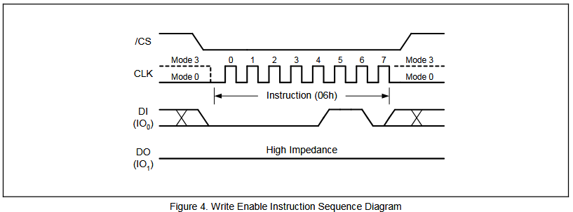
The Write Enable instruction 0x06 must be sent before write and erase commands will be accepted. This prevents accidental erasures or overwrites of your valuable data.
- CS pin is pulled low
- Write the Write Enable instruction
0x06 - CS pin is pulled high
This command must be sent immediately before any write, erase or configuration command.
SPI> [0x06]

CS Enabled
TX: 0x06
CS Disabled
SPI>
[- Start of SPI transaction. Lowers the CS pin to ground.0x06- Write Enable instruction.]- End of SPI transaction. Raises the CS pin to 3.3volts.
Verify write enable
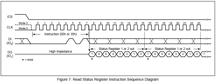
The Read Status Register instruction 0x05 can be used to verify that the ‘Write Enable’ instruction was correctly received. The status register is a single byte that contains several flags.
- CS pin is pulled low
- Write the Read Status Register instruction
0x05 - Read the status register byte
- CS pin is pulled high
SPI> [0x05 r]

CS Enabled
TX: 0x05
RX: 0x02
CS Disabled
SPI>
Let’s read and decode the status register.
[- Start of SPI transaction. Lowers the CS pin to ground.0x05- Read Status Register instruction.r- Read 1 byte.]- End of SPI transaction. Raises the CS pin to 3.3volts.
The status register value is 0x02.
SPI> = 0x02
 =0x02 =2 =0b00000010
SPI>
We can convert the status register value to binary to see which bits are set using the Bus Pirate = convert command.
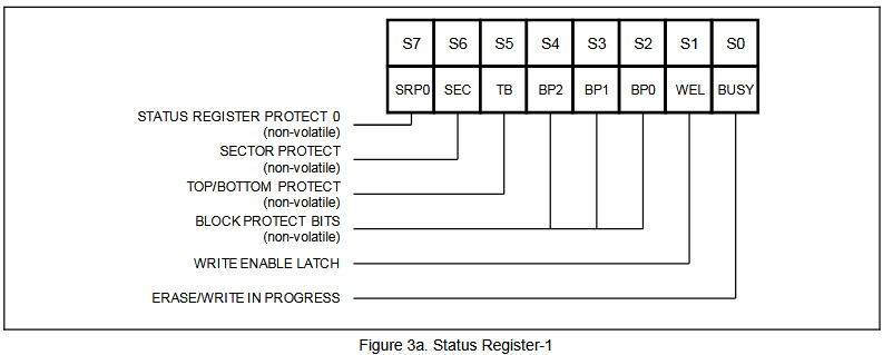
We’re interested in bit S1, the write enable latch (WEL). WEL is set to 1 when the Write Enable instruction is received. WEL is 1 (0b00000010) so we’re ready to write some data!
Erase sector
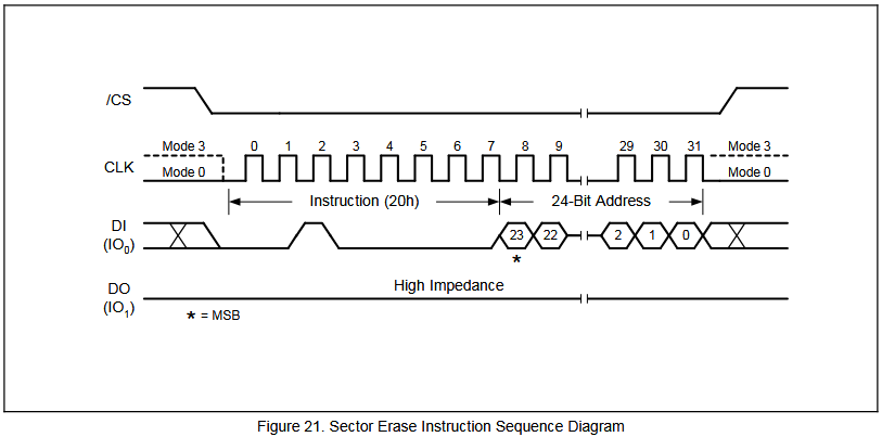
Flash works by flipping 1s in the memory to 0. Writing a location twice will simply flip more bits from 1 to 0, but will not flip 0 to 1. The erase sector command 0x20 is used to flip all bits in a 4096 byte sector from 0 to 1, then we can write new data.
- CS pin is pulled low
- Write the Sector Erase instruction
0x20 - Write the 3 byte address of the first byte in the sector to erase
- CS pin is pulled high
The erase sector command is followed by a three byte address of the location to begin erasing 4096 bytes. It’s not possible to erase across sector boundaries. The 4096 byte sectors are ‘aligned’ in bocks. The first sector begins at 0, the next at 4096, the next at 8192 and so on.
Sector erase resets all bits to 1 in a 4096 byte sector. It is not possible to erase just a single byte in most NOR flash chips. It’s part of what makes them so cheap!
SPI> [0x06] [0x20 0x00 0x00 0x00]

CS Enabled
TX: 0x06
CS Disabled
CS Enabled
TX: 0x20 0x00 0x00 0x00
CS Disabled
SPI>
We’ll erase the first sector from byte 0 to byte 4095. A write enable command must be sent before the erase sector command will be accepted.
[0x06]- Write Enable instruction (see Enable Writes).[- Start of SPI transaction. Lowers the CS pin to ground.0x20- Erase Sector instruction.0x00 0x00 0x00- Address 0x00.]- End of SPI transaction. Raises the CS pin to 3.3volts.
Verify erase sector
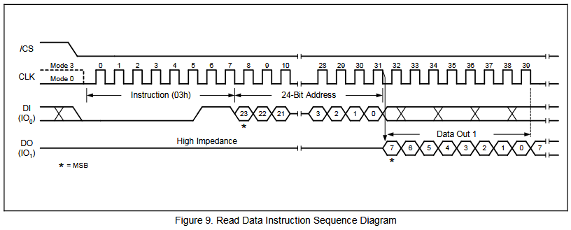
The Read Data instruction 0x03 can be used to verify that the sector has been erased. The read data command is followed by a three byte address where we’ll start reading.
- CS pin is pulled low
- Write the Read Data instruction
0x03 - Write the 3 byte address of the first byte to read
- Read data, up to the full size of the flash chip
- CS pin is pulled high
SPI> [0x03 0x00 0x00 0x00 r:256]

CS Enabled
TX: 0x03 0x00 0x00 0x00
RX: 0xFF 0xFF 0xFF 0xFF 0xFF 0xFF 0xFF 0xFF
    0xFF 0xFF 0xFF 0xFF 0xFF 0xFF 0xFF 0xFF
    0xFF 0xFF 0xFF 0xFF 0xFF 0xFF 0xFF 0xFF
    0xFF 0xFF 0xFF 0xFF 0xFF 0xFF 0xFF 0xFF
    0xFF 0xFF 0xFF 0xFF 0xFF 0xFF 0xFF 0xFF
    0xFF 0xFF 0xFF 0xFF 0xFF 0xFF 0xFF 0xFF
    0xFF 0xFF 0xFF 0xFF 0xFF 0xFF 0xFF 0xFF
    0xFF 0xFF 0xFF 0xFF 0xFF 0xFF 0xFF 0xFF
    0xFF 0xFF 0xFF 0xFF 0xFF 0xFF 0xFF 0xFF
    0xFF 0xFF 0xFF 0xFF 0xFF 0xFF 0xFF 0xFF
    0xFF 0xFF 0xFF 0xFF 0xFF 0xFF 0xFF 0xFF
    0xFF 0xFF 0xFF 0xFF 0xFF 0xFF 0xFF 0xFF
    0xFF 0xFF 0xFF 0xFF 0xFF 0xFF 0xFF 0xFF
    0xFF 0xFF 0xFF 0xFF 0xFF 0xFF 0xFF 0xFF
    0xFF 0xFF 0xFF 0xFF 0xFF 0xFF 0xFF 0xFF
    0xFF 0xFF 0xFF 0xFF 0xFF 0xFF 0xFF 0xFF
    0xFF 0xFF 0xFF 0xFF 0xFF 0xFF 0xFF 0xFF
    0xFF 0xFF 0xFF 0xFF 0xFF 0xFF 0xFF 0xFF
    0xFF 0xFF 0xFF 0xFF 0xFF 0xFF 0xFF 0xFF
    0xFF 0xFF 0xFF 0xFF 0xFF 0xFF 0xFF 0xFF
    0xFF 0xFF 0xFF 0xFF 0xFF 0xFF 0xFF 0xFF
    0xFF 0xFF 0xFF 0xFF 0xFF 0xFF 0xFF 0xFF
    0xFF 0xFF 0xFF 0xFF 0xFF 0xFF 0xFF 0xFF
    0xFF 0xFF 0xFF 0xFF 0xFF 0xFF 0xFF 0xFF
    0xFF 0xFF 0xFF 0xFF 0xFF 0xFF 0xFF 0xFF
    0xFF 0xFF 0xFF 0xFF 0xFF 0xFF 0xFF 0xFF
    0xFF 0xFF 0xFF 0xFF 0xFF 0xFF 0xFF 0xFF
    0xFF 0xFF 0xFF 0xFF 0xFF 0xFF 0xFF 0xFF
    0xFF 0xFF 0xFF 0xFF 0xFF 0xFF 0xFF 0xFF
    0xFF 0xFF 0xFF 0xFF 0xFF 0xFF 0xFF 0xFF
    0xFF 0xFF 0xFF 0xFF 0xFF 0xFF 0xFF 0xFF
    0xFF 0xFF 0xFF 0xFF 0xFF 0xFF 0xFF 0xFF

CS Disabled
SPI>
We’ll read the first 256 bytes from address 0x000000, all the bytes should be erased and set to 0xFF.
[- Start of SPI transaction. Lowers the CS pin to ground.0x03- Read Data instruction.0x00 0x00 0x00- Start reading at address 0x000000.r:256- Read 256 bytes.]- End of SPI transaction. Raises the CS pin to 3.3volts.
The 256 bytes read are all 0xFF, the sector was successfully erased.
Enable writes and verify
SPI> [0x06] [0x05 r]

CS Enabled
TX: 0x06
CS Disabled
CS Enabled
TX: 0x05
RX: 0x02
CS Disabled
SPI> = 0x02
 =0x02 =2 =0b00000010
SPI>
Use the write enable instruction 0x06 to enable writes. Verify the write enable bit is set to 1 (0x02=0b00000010) using the read status register instruction 0x05. We can do this all on a single line.
[0x06] [0x05 r]- Write Enable instruction followed by Read Status Register instruction. The response is the status register byte.= 0x02- Convert the status register value to binary. The write enable latch bit (0b00000010) should be set to 1.
Write data
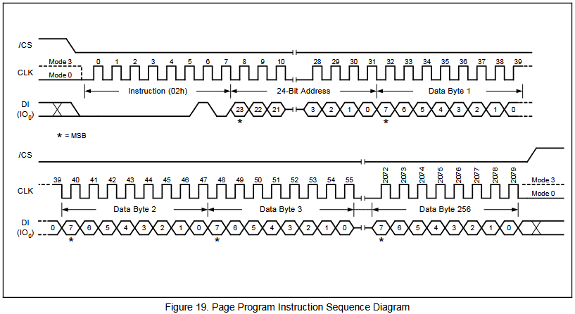
The Page Program instruction 0x02 is used to write data to the flash chip. The smallest unit of data that can be written is a page, which is 256 bytes.
- CS pin is pulled low
- Write the Page Program instruction
0x02 - Write the 3 byte address of the first location to write
- Write 256 bytes of data
- CS pin is pulled high
The smallest unit of data that can be written is a page, which is 256 bytes. The smallest unit of data that can be erased is a sector, which is 4096 bytes. It is not possible to write or erase a single byte in most NOR flash chips. Juggling these constraints can be tricky!
SPI> [0x06] [0x02 0x00 0x00 0x00 0xAA:256]

CS Enabled
TX: 0x06
CS Disabled
CS Enabled
TX: 0x02 0x00 0x00 0x00 0xAA 0xAA 0xAA 0xAA
    0xAA 0xAA 0xAA 0xAA 0xAA 0xAA 0xAA 0xAA
    0xAA 0xAA 0xAA 0xAA 0xAA 0xAA 0xAA 0xAA
    0xAA 0xAA 0xAA 0xAA 0xAA 0xAA 0xAA 0xAA
    0xAA 0xAA 0xAA 0xAA 0xAA 0xAA 0xAA 0xAA
    0xAA 0xAA 0xAA 0xAA 0xAA 0xAA 0xAA 0xAA
    0xAA 0xAA 0xAA 0xAA 0xAA 0xAA 0xAA 0xAA
    0xAA 0xAA 0xAA 0xAA 0xAA 0xAA 0xAA 0xAA
    0xAA 0xAA 0xAA 0xAA 0xAA 0xAA 0xAA 0xAA
    0xAA 0xAA 0xAA 0xAA 0xAA 0xAA 0xAA 0xAA
    0xAA 0xAA 0xAA 0xAA 0xAA 0xAA 0xAA 0xAA
    0xAA 0xAA 0xAA 0xAA 0xAA 0xAA 0xAA 0xAA
    0xAA 0xAA 0xAA 0xAA 0xAA 0xAA 0xAA 0xAA
    0xAA 0xAA 0xAA 0xAA 0xAA 0xAA 0xAA 0xAA
    0xAA 0xAA 0xAA 0xAA 0xAA 0xAA 0xAA 0xAA
    0xAA 0xAA 0xAA 0xAA 0xAA 0xAA 0xAA 0xAA
    0xAA 0xAA 0xAA 0xAA 0xAA 0xAA 0xAA 0xAA
    0xAA 0xAA 0xAA 0xAA 0xAA 0xAA 0xAA 0xAA
    0xAA 0xAA 0xAA 0xAA 0xAA 0xAA 0xAA 0xAA
    0xAA 0xAA 0xAA 0xAA 0xAA 0xAA 0xAA 0xAA
    0xAA 0xAA 0xAA 0xAA 0xAA 0xAA 0xAA 0xAA
    0xAA 0xAA 0xAA 0xAA 0xAA 0xAA 0xAA 0xAA
    0xAA 0xAA 0xAA 0xAA 0xAA 0xAA 0xAA 0xAA
    0xAA 0xAA 0xAA 0xAA 0xAA 0xAA 0xAA 0xAA
    0xAA 0xAA 0xAA 0xAA 0xAA 0xAA 0xAA 0xAA
    0xAA 0xAA 0xAA 0xAA 0xAA 0xAA 0xAA 0xAA
    0xAA 0xAA 0xAA 0xAA 0xAA 0xAA 0xAA 0xAA
    0xAA 0xAA 0xAA 0xAA 0xAA 0xAA 0xAA 0xAA
    0xAA 0xAA 0xAA 0xAA 0xAA 0xAA 0xAA 0xAA
    0xAA 0xAA 0xAA 0xAA 0xAA 0xAA 0xAA 0xAA
    0xAA 0xAA 0xAA 0xAA 0xAA 0xAA 0xAA 0xAA
    0xAA 0xAA 0xAA 0xAA 0xAA 0xAA 0xAA 0xAA
    0xAA 0xAA 0xAA 0xAA
CS Disabled
SPI>
Use the page program command 0x02 to write 256 bytes of data to address 0x00. The command is followed by a three byte address of the location to begin writing 256 bytes 0x00 0x00 0x00. The data to be written i (0x69) follows the address.
[0x06]- Write Enable instruction (see Enable Writes).[- Start of SPI transaction. Lowers the CS pin to ground.0x02- Page Program instruction.0x00 0x00 0x00- Address to begin writing: 0x000000.0xAA:256- Write 256 bytes of0xAA.]- End of SPI transaction. Raises the CS pin to 3.3volts.
Write up to 256 bytes at a time. If more than 256 bytes are sent, the internal buffer will circle back to the beginning of the page and overwrite previously sent data.
Read data
SPI> [0x03 0x00 0x00 0x00 r:256]

CS Enabled
TX: 0x03 0x00 0x00 0x00
RX: 0xAA 0xAA 0xAA 0xAA 0xAA 0xAA 0xAA 0xAA
    0xAA 0xAA 0xAA 0xAA 0xAA 0xAA 0xAA 0xAA
    0xAA 0xAA 0xAA 0xAA 0xAA 0xAA 0xAA 0xAA
    0xAA 0xAA 0xAA 0xAA 0xAA 0xAA 0xAA 0xAA
    0xAA 0xAA 0xAA 0xAA 0xAA 0xAA 0xAA 0xAA
    0xAA 0xAA 0xAA 0xAA 0xAA 0xAA 0xAA 0xAA
    0xAA 0xAA 0xAA 0xAA 0xAA 0xAA 0xAA 0xAA
    0xAA 0xAA 0xAA 0xAA 0xAA 0xAA 0xAA 0xAA
    0xAA 0xAA 0xAA 0xAA 0xAA 0xAA 0xAA 0xAA
    0xAA 0xAA 0xAA 0xAA 0xAA 0xAA 0xAA 0xAA
    0xAA 0xAA 0xAA 0xAA 0xAA 0xAA 0xAA 0xAA
    0xAA 0xAA 0xAA 0xAA 0xAA 0xAA 0xAA 0xAA
    0xAA 0xAA 0xAA 0xAA 0xAA 0xAA 0xAA 0xAA
    0xAA 0xAA 0xAA 0xAA 0xAA 0xAA 0xAA 0xAA
    0xAA 0xAA 0xAA 0xAA 0xAA 0xAA 0xAA 0xAA
    0xAA 0xAA 0xAA 0xAA 0xAA 0xAA 0xAA 0xAA
    0xAA 0xAA 0xAA 0xAA 0xAA 0xAA 0xAA 0xAA
    0xAA 0xAA 0xAA 0xAA 0xAA 0xAA 0xAA 0xAA
    0xAA 0xAA 0xAA 0xAA 0xAA 0xAA 0xAA 0xAA
    0xAA 0xAA 0xAA 0xAA 0xAA 0xAA 0xAA 0xAA
    0xAA 0xAA 0xAA 0xAA 0xAA 0xAA 0xAA 0xAA
    0xAA 0xAA 0xAA 0xAA 0xAA 0xAA 0xAA 0xAA
    0xAA 0xAA 0xAA 0xAA 0xAA 0xAA 0xAA 0xAA
    0xAA 0xAA 0xAA 0xAA 0xAA 0xAA 0xAA 0xAA
    0xAA 0xAA 0xAA 0xAA 0xAA 0xAA 0xAA 0xAA
    0xAA 0xAA 0xAA 0xAA 0xAA 0xAA 0xAA 0xAA
    0xAA 0xAA 0xAA 0xAA 0xAA 0xAA 0xAA 0xAA
    0xAA 0xAA 0xAA 0xAA 0xAA 0xAA 0xAA 0xAA
    0xAA 0xAA 0xAA 0xAA 0xAA 0xAA 0xAA 0xAA
    0xAA 0xAA 0xAA 0xAA 0xAA 0xAA 0xAA 0xAA
    0xAA 0xAA 0xAA 0xAA 0xAA 0xAA 0xAA 0xAA
    0xAA 0xAA 0xAA 0xAA 0xAA 0xAA 0xAA 0xAA

CS Disabled
SPI>
Use the Read Data instruction 0x03 once again to confirm the page was filled with 0xA0.
[- Start of SPI transaction. Lowers the CS pin to ground.0x03- Read Data instruction.0x00 0x00 0x00- Address to begin reading: 0x00.r:256- Read 256 bytes of data.]- End of SPI transaction. Raises the CS pin to 3.3volts.
All 256 bytes read are 0xAA, the page was successfully written.
If the writing/reading process fails, check all connections. /HOLD & /WP pins must be connected to 3.3 volts.
flash command
The flash command can read, write, and erase common SPI flash memory chips directly in the Bus Pirate terminal. The Serial Flash Universal Driver at the heart of the flash command attempts to identify the flash chip by reading the SFDP tables. If a chip doesn’t have SFDP tables, the driver has a database of common chips to fall back on.
Get a Bus Pirate
Get Bus Pirate & Accessories
- Browse Complete Bus Pirate hardware collection
- Bus Pirate 5 REV10 with enclosure
- Probe Cable Kit
- Auxiliary Cable Kit
- Quick Connect Adapter