MB85RC256V FRAM memory I2C

FRAM (ferroelectric RAM) is a non-volatile memory that combines the speed of SRAM with the persistence of EEPROM. It’s pretty new and much more expensive than EEPROM or flash, but check out these benefits:
- Does not require a power supply to retain data
- Writes are “instant”, no need to poll until the write is complete
- 10^12 write cycles, 1 million times more than EEPROM
- 200uA operating current vs 1mA for EEPROM
- Page size is the entire chip, no juggling 8, 16 or 64 byte write pages!
The Fujitsu MB85RC256V is a 256Kbit (32Kbyte) FRAM memory chip with an I2C interface.
Get Bus Pirate & Accessories
Connections
| Bus Pirate | MB85RC256V | Description |
|---|---|---|
| IO0/SDA | SDA (5) | I2C Data |
| IO1/SCL | SCL (6) | I2C Clock |
| Vout | VDD (8) | 3.3 volt power supply |
| GND | VSS (4) | Ground |
Connect the Bus Pirate to the FRAM as shown in the table above.
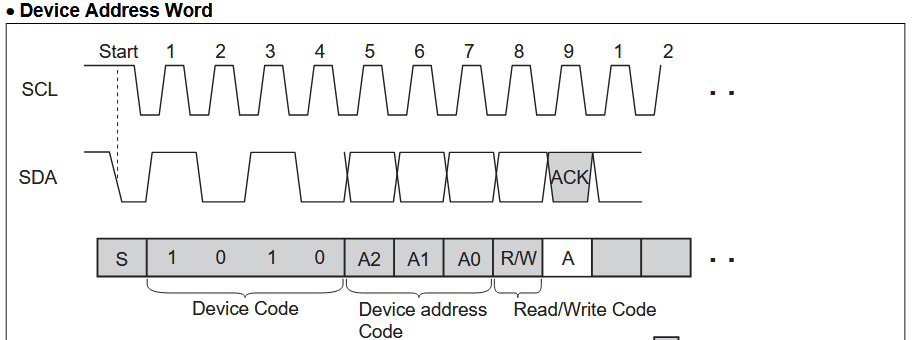
In addition to the I2C and power connections, the MB85RC256V three address pins and a write protect pin (protection active when WP is high/1).
The base I2C address is 0b1010, while A0, A1 and A2 set the lower 3 bits of the address. To use multiple chips on the same I2C bus, connect one or more of the address pins to VDD to give each a unique I2C address.
The address and write protect pins have internal pull-down resistors. By default the I2C address is 0b1010000, and write protection is disabled. Fujitsu was so considerate to include internal pull-downs on the pins, we don’t need to set them with external components!
See it in action
Setup
HiZ> m i2c

Mode: I2C
I2C speed
 1kHz to 1000kHz
 x. Exit
kHz (400kHz*) > 400
Clock stretching
 1. OFF*
 2. ON
 x. Exit
OFF (1) > 1
I2C>
This particular FRAM chip has an I2C interface with a top speed of 1MHz, though others have an SPI interface with a higher top speed.
While the FRAM has a top speed of 1MHz, 400kHz is more reliable when the device is connected to a breadboard or long wires.
Power supply
Despite being a modern chip, the FRAM still has a maximum supply of up to 5 volts. This is probably part of making it a drop-in replacement for the older EEPROMs.
I2C> W 3.3
3.30V requested, closest value: 3.30V
300.0mA requested, closest value: 300.0mA

Power supply:Enabled
Vreg output: 3.3V, Vref/Vout pin: 3.3V, Current: 2.6mA

I2C>
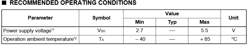
Any voltage between 2.7 and 5.5 volts is acceptable. Let’s go with the present standard of 3.3 volts.
W 3.3- enable the onboard power supply at 3.3 volts.
Images source: datasheet.
Pull-up resistors
I2C> P
Pull-up resistors: Enabled (10K ohms @ 3.3V)

I2C>
I2C is an open collector output bus, the Bus Pirate and the FRAM can only pull the line low to 0 (ground). A pull-up resistor is needed to pull the line high to 1 (3.3 volts). The Bus Pirate has built-in pull-up resistors that can be enabled with the P command.
P- Enable the onboard pull-up resistors.
Be sure to enable the pull-up resistors. The data line will never go high without them and you’ll read only 0s.
I2C address scan
I2C> scan
I2C address search:
0x50 (0xA0 W) (0xA1 R)
0x7C (0xF8 W)

Found 3 addresses, 1 W/R pairs.

I2C>
Let’s see if we can find the FRAM I2C address. We could look in the datasheet, or we can be lazy and run an I2C address scan.
scan- Scan the I2C bus for devices
The scanner found an I2C device at address 0x50 (0xA0 write, 0xA1 read). That’s the FRAM main interface. The second write address 0x7c (0xf8 write) is used to get the device ID, which we’ll do later.
If the scanner doesn’t find the device, ensure the power supply is enabled W 3.3 and the pull-up resistors are enabled P.
Write & Read Bytes
FRAM can read and write single bytes of data anywhere in the 32 Kbyte memory range.
Write Byte
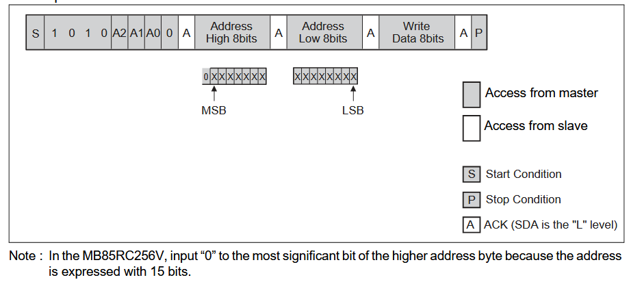
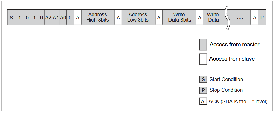
Writing to the FRAM is identical to writing a 24Cxxx EEPROM. The write sequence is as follows:
- I2C START bit - begins an I2C transaction
- The I2C write address 0xA0 (Device Address + Write bit)
- Two byte address of the location to write in the 32 Kbytes of FRAM
- The data to write
- I2C STOP bit - ends the transaction
The address is two bytes representing a location from 0 to 32767 (0x0000 to 0x7FFF) in the memory array. The first byte is the high byte, the second byte is the low byte.
I2C> [0xa0 0x00 0x09 0x48]

I2C START
TX: 0xA0 ACK 0x00 ACK 0x09 ACK 0x48 ACK
I2C STOP
I2C>
Let’s write byte 0x48 to the FRAM at address 0x0009 (9). The address is two bytes, so we send 0x00 0x09 for the high and low bytes.
[- I2C START bit0xa0- I2C address and write bit0x00 0x09- Set write location to address 0x0009 (9)0x48- Data to write]- I2C STOP bit
Unlike EEPROM and flash memory, FRAM does not require a write delay. The write is “instant” and the data is immediately available to read.
ACK means the FRAM chip acknowledged each byte. If you see NACK, it means the chip did not acknowledge the command and the write failed. If you see a NACK, check the connections, power supply, and pull-up resistors.
Read Byte
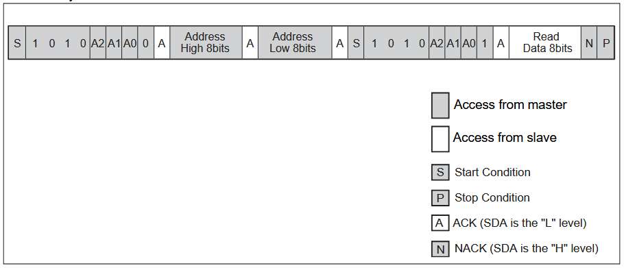
Reading a byte is a two step process.
- Set the location to read with a command to the write address (0xA0). This is the same sequency as writing a byte, but we don’t include any data (sometimes called a Dummy Write).
- Send the read address (0xA1) and read data from the EEPROM.
Reading from most I2C devices is a two step process. First we set the address pointer, then we read the data. This is a common pattern in I2C devices.
Set address pointer
I2C> [0xa0 0x00 0x09]

I2C START
TX: 0xA0 ACK 0x00 ACK 0x09 ACK
I2C STOP
I2C>
A 0xa0 write command is used to set the address pointer to 0x0009. This time we won’t include any data. The address pointer will be updated, but nothing is written to the FRAM.
[- I2C START bit0xa0- I2C address and write bit0x00 0x09- address pointer, high and low bytes, set to 0x0009 (9)]- I2C STOP bit
The address pointer has been set to 0x0009, the location of the data we want to read. This command didn’t include a data byte, so nothing was written to the FRAM.
Read Data
I2C> [0xa1 r]

I2C START
TX: 0xA1 ACK
RX: 0x48 NACK
I2C STOP
I2C>
Now that the address pointer is set to 0x0009, we can read the data at that location using the I2C read address 0xa1.
[- I2C START bit0xa1- I2C address and read bitr- Read 1 byte]- I2C STOP bit
The data read from the EEPROM (RX) is 0x48, the same value we wrote earlier.
We used two discrete commands to set the address pointer and read the data. This could also be done in a single sequence by omitting the I2C STOP bit between the two commands. This is called a “repeated start” and is the method shown in the diagram above. The command would look like this: [0xa0 0x00 0x09 [ 0xa1 r]. The I2C STOP bit is not needed between the two commands, but it is required at the end of the transaction.
Write & Read Multiple Bytes
EEPROM and flash memory is organized into write pages of 8, 16, or 64 bytes. This means that writes must be aligned to the page size and boundary, and then you wait for the write to complete.
FRAM does not have this limitation! This is a huge advantage that we just learned about at this moment! Writing to FRAM is like writing to SRAM, you can write as much data wherever you want at top speed without juggling around page boundaries. This makes code much simpler!
MB85RC256V FRAM doesn’t have a write page size like traditional EEPROM and flash memory.
Write Multiple Bytes
Writing multiple bytes is similar to writing single byte, we just send more data! Set the address pointer to the location of the first byte to write, and then send as much data as you like.
Note that when the address pointer reaches the end of the 32 Kbyte memory, it rolls over and starts writing at the beginning (0x0000) of the memory.
I2C> [0xa0 0x00 0x00 0x55:16 0xaa:16]

I2C START
TX: 0xA0 ACK 0x00 ACK 0x00 ACK 0x55 ACK 0x55 ACK 0x55 ACK 0x55 ACK 0x55 ACK
    0x55 ACK 0x55 ACK 0x55 ACK 0x55 ACK 0x55 ACK 0x55 ACK 0x55 ACK 0x55 ACK
    0x55 ACK 0x55 ACK 0x55 ACK 0xAA ACK 0xAA ACK 0xAA ACK 0xAA ACK 0xAA ACK
    0xAA ACK 0xAA ACK 0xAA ACK 0xAA ACK 0xAA ACK 0xAA ACK 0xAA ACK 0xAA ACK
    0xAA ACK 0xAA ACK 0xAA ACK
I2C STOP
I2C>
Let’s write 32 bytes starting at address 0x0000, the beginning of the memory.
[- I2C START bit0xa0- I2C address and write bit0x00 0x00- set the address pointer to 0x0000 (the beginning of the memory)0x55:16 0xaa:16- Write 0x55 and 0xaa to the FRAM, 16 times each]- I2C STOP bit
Remember two big advantages of FRAM:
No write delay, the data is immediately available to read
No page size, you can write as much data as you like without worrying about page boundaries
Read Multiple Bytes
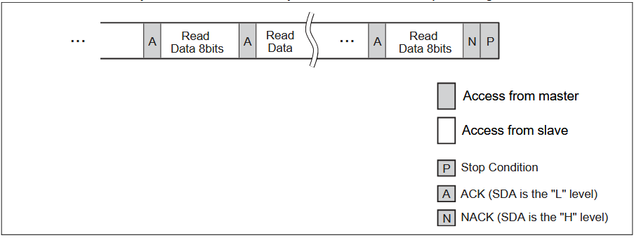
Reading multiple bytes is similar to reading a single byte. First we set the address pointer to the beginning of the page with a write command, then we read the data - only more of it! The last byte read is NACKed by the Bus Pirate automatically to tell the FRAM we’re done reading.
Set Address Pointer
I2C> [0xa0 0x00 0x00]

I2C START
TX: 0xA0 ACK 0x00 ACK 0x00 ACK
I2C STOP
I2C>
Set the address pointer to the beginning the memory, address 0x0000.
[- I2C START bit0xa0- I2C address and write bit0x00 0x00- set the address pointer to 0x0000 (the beginning of the memory)]- I2C STOP bit
Read Bytes
I2C> [0xa1 r:32]

I2C START
TX: 0xA1 ACK
RX: 0x55 ACK 0x55 ACK 0x55 ACK 0x55 ACK 0x55 ACK 0x55 ACK 0x55 ACK 0x55 ACK
    0x55 ACK 0x55 ACK 0x55 ACK 0x55 ACK 0x55 ACK 0x55 ACK 0x55 ACK 0x55 ACK
    0xAA ACK 0xAA ACK 0xAA ACK 0xAA ACK 0xAA ACK 0xAA ACK 0xAA ACK 0xAA ACK
    0xAA ACK 0xAA ACK 0xAA ACK 0xAA ACK 0xAA ACK 0xAA ACK 0xAA ACK 0xAA NACK

I2C STOP
I2C>
Read back 32 bytes to verify the data was written.
[- I2C START bit0xa1- I2C address and read bitr:32- Read 32 bytes]- I2C STOP bit
The data read from the FRAM (RX) is 16 bytes of 0x55 and 16 bytes of 0xaa. The write was successful!
Read FRAM ID
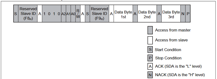
The MB85RC256V has a 3 byte device ID that can be read from the Reserved Slave ID (0xf8/0xf9), a second I2C address that is not used for normal operations.
- I2C START bit - begins an I2C transaction
- Write to the Reserved Slave ID write address (0xf8)
- Write the I2C device address (0xa0 or 0xa1, doesn’t matter)
- I2C repeated START bit - prepares to read data
- Write the Reserved Slave ID read address (0xf9)
- Read 3 byte device ID
- I2C STOP bit - ends the transaction
I2C> [0xf8 0xa0 [0xf9 r:3]

I2C START
TX: 0xF8 ACK 0xA0 ACK
I2C REPEATED START
TX: 0xF9 ACK
RX: 0x00 ACK 0xA5 ACK 0x10 NACK
I2C STOP
I2C>
[0xf8 0xa0 [0xf9 r:3]- Read the 3 byte device ID from the Reserved Slave ID address.
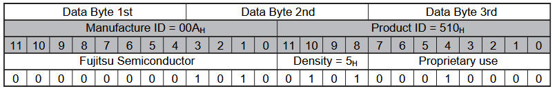
The device ID is 0x00A510.
- The upper 12 bits (0x00A) make up the manufacturer ID, Fujitsu.
- The lower 12 bits (0x510) make up the product ID, which includes a 4 bit density code (0x5) and a byte of proprietary info (0x10).
Get a Bus Pirate
Get Bus Pirate & Accessories
- Browse Complete Bus Pirate hardware collection
- Bus Pirate 5 REV10 with enclosure
- Probe Cable Kit
- Auxiliary Cable Kit
- Quick Connect Adapter