Identify Serial EEPROM, Flash and FRAM chips
Documentation still in progress. Todo:
Photographs of common chip markings
The Bus Pirate eeprom and flash commands can read, write, erase, verify and test many common serial memory chips: SPI Flash (25Q), SPI EEPROM (25x, 95x), I2C EEPROM (24x), 1-Wire EEPROM, Microwire EEPROM (93x), SPI FRAM and I2C FRAM.
This page will help you identify the type of serial memory chip you have, the pinout, and the voltage requirements.
Types of Serial memory supported
| Type | Part Number* | Ex. Part Num. | Example Manufacturers |
|---|---|---|---|
| SPI Flash | 25Qnnn | W25Q128 | Winbond, Micron, GigaDevice, PUYA |
| SPI EEPROM | 25xnnn, 95xnnn | 25LC040, AT25040 | Microchip, Atmel, STMicroelectronics |
| I2C EEPROM | 24xnnn | 24LC20, AT24C02 | Microchip, Atmel, STMicroelectronics |
| 1-Wire EEPROM | 243n | DS2341, GX2341, DS24B33 | Dallas/Maxim, GX |
| Microwire EEPROM | 93xnn | AT93C46, 93LC56C | Microchip, Atmel, STMicroelectronics |
| SPI FRAM | FM25xnnn, MB85Xnnn | FM25CL64B, MB85RS512 | Ramxeed (Fujitsu), Infineon, ROHM |
| I2C FRAM | FM24xnnn, MB85Xnnn | FM24CL64B, MB85RC64 | Ramxeed (Fujitsu), Infineon, ROHM |
*n = device size in Kbits, usually.
SPI Flash Memory
SPI Flash chips use NOR memory, which is cheap, fast, and small. There are several trade offs though:
- Size: 1 Mbit to 512 Mbit (128K - 64M)
- Read: Not byte addressable, data must be read in whole pages (usually 256 bytes) at a time.
- Write: Not byte addressable, data must be written in whole pages (usually 256 bytes) at a time and page aligned.
- Erase: Data must be erased in whole sectors (usually 4K, 8K or 64K) at a time.
- Cost: SPI Flash is cheap!
- Write cycles: 10,000+
- Data retention: 20 years
To update existing data, you must first read all the data in the erase sector, modify it in RAM, erase the whole 4K sector, and then write it back to the flash memory.
Identifying SPI Flash chips
A really common SPI Flash chip is the Winbond W25Qnnn series. It will be labeled with the Winbond logo and the part number will start with “W25Q” followed by a three digit number indicating the size in Mbits.
Most recent SPI flash chips have their characteristics stored in JEDEC standard SFDP (Serial Flash Discoverable Parameters) format. The flash command in SPI mode will automatically read the SFDP data and display the chip characteristics, including the manufacturer, size, erase sector size, and other parameters.
If SFDP data isn’t available, the flash command has a database of known chips and can identify them by their JEDEC ID.
The flash command in SPI mode can probe, read, write, erase, verify and test most SPI flash chips.
SPI Flash pinout
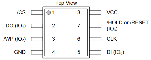
| Pin | Name | Description | Pin | Name | Description | |
|---|---|---|---|---|---|---|
| 1 | CS | SPI Chip Select (active low) | 8 | VCC | Power supply | |
| 2 | SO | SPI Serial Out (MISO) | 7 | HOLD | Hold (active low)* | |
| 3 | WP | Write Protect (active low)* | 6 | SCK | SPI Serial Clock | |
| 4 | GND | Ground | 5 | SI | SPI Serial In (MOSI) |
Write protect pin
The write protect pin is optional, and may not be present on all chips. If it is present, it is used to protect the chip from being written to. If the pin is connected to ground, the chip can be written to. If the pin is connected to VCC, the chip is write protected and cannot be written to.
Hold pin
The hold pin is also optional, and may not be present on all chips. If it is present, it is used to pause the chip’s operation without resetting it. If the pin is connected to ground, the chip will pause its operation until the pin is released.
Image source: Winbond W25Q128JV datasheet
SPI Flash voltage requirements
| Family | Minimum Voltage | Maximum Voltage |
|---|---|---|
| W25Q | 2.7V | 3.6V |
Most SPI Flash chips will work at 3.3V, but some newer chips may have a lower maximum voltage. Always check the datasheet for the specific chip you are using if possible.
EEPROM memory
Unlike Flash (NOR) memory, EEPROM memory is byte-addressable and can be written to one byte at a time.
- Size: 1Kbit to 4 Mbit (128B - 512K)
- Read: Byte addressable, can read any byte in the chip.
- Write: 1 byte up to the page size (8 to 256 bytes, depending on chip) at a time. Writes must be aligned to the page size.
- Erase: No separate erase process is needed, bytes are erased individually before writing.
- Cost: EEPROM is generally more expensive than NOR Flash memory.
- Write cycles: 1,000,000+
- Data retention: 100-200 years
Identifying SPI EEPROM chips
SPI EEPROM chips are usually labeled with a part number starting with “25” or “95”. The “25” series is more common and includes chips like AT25C020, 25LC040, 25AA080, etc. The “95” series is STM’s name for their 25x compatible EEPROMs, just substitute the same sized 25x part, e.g. 25LC040 is equivalent to 95LC040.
The eeprom command in SPI mode can probe, read, write, erase, verify and test most SPI EEPROM chips.
| Device | Density | Size (bytes) | Page Size (Bytes) | Address Bytes | Block Select Bits | B.S. Offset |
|---|---|---|---|---|---|---|
| 25X010 | 1 Kbit | 128 | 8(AT)/16 | 1 | 0 | |
| 25X020** | 2 Kbit | 256 | 8(AT)/16 | 1 | 0 | |
| 25X040** | 4 Kbit | 512 | 8(AT)/16 | 1 | 1 | 3 |
| 25X080 | 8 Kbit | 1024 | 16/32(AT,STM) | 2 | 0 | |
| 25X160 | 16 Kbit | 2048 | 16/32(AT,STM) | 2 | 0 | |
| 25X320** | 32 Kbit | 4096 | 32 | 2 | 0 | |
| 25X640** | 64 Kbit | 8192 | 32 | 2 | 0 | |
| 25X128** | 128 Kbit | 16384 | 64 | 2 | 0 | |
| 25X256** | 256 Kbit | 32768 | 64 | 2 | 0 | |
| 25X512** | 512 Kbit | 65536 | 128 | 2 | 0 | |
| 25XM01, 25X1024** | 1 Mbit | 131072 | 256 | 3 | 0 | |
| 25XM02 | 2 Mbit | 262144 | 256 | 3 | 0 | |
| 25XM04** | 4 Mbit | 524288 | 256/512(STM) | 3 | 0 |
**Tested devices
25x/95x chips have a variety of part numbers, but tend to operate in the same way. Often a manufacturer specific part number indicates a different voltage range or upgraded features. AT25, 25LC, 25AA, 25CS and M95 are all part of same basic 25x family of chips.
SPI EEPROM pinout
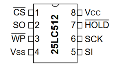
| Pin | Name | Description | Pin | Name | Description | |
|---|---|---|---|---|---|---|
| 1 | CS | SPI Chip Select (active low) | 8 | VCC | Power supply | |
| 2 | SO | SPI Serial Out (MISO) | 7 | HOLD | Hold (active low)* | |
| 3 | WP | Write Protect (active low)* | 6 | SCK | SPI Serial Clock | |
| 4 | GND | Ground | 5 | SI | SPI Serial In (MOSI) |
Write protect pin
The write protect pin is optional, and may not be present on all chips. If it is present, it is used to protect the chip from being written to. If the pin is connected to ground, the chip can be written to. If the pin is connected to VCC, the chip is write protected and cannot be written to.
Hold pin
The hold pin is also optional, and may not be present on all chips. If it is present, it is used to pause the chip’s operation without resetting it. If the pin is connected to ground, the chip will pause its operation until the pin is released.
Image source: Microchip 25x512 datasheet
SPI EEPROM voltage requirements
| 25x/95x Family | Minimum Voltage | Maximum Voltage | |
|---|---|---|---|
| AT25 | 1.8V | 5.5V | |
| 25LC | 2.5V | 5.5V | |
| 25AA | 1.8V | 5.5V | |
| 25CS | 1.7V | 5.5V | |
| M95 | 2.5V | 5.5V |
3.3 volts is a good voltage to use with most 25x/95x chips, but a few newer chips may have a lower maximum voltage. Always check the datasheet for the specific chip you are using if possible.
Identifying I2C EEPROM chips
I2C EEPROM chips are usually labeled with a part number starting with “24”. The “24” series includes chips like 24LC02, 24AA04, AT2402 etc. The “24” series is the most common I2C EEPROM series.
The eeprom command in I2C mode can probe, read, write, erase, verify and test most I2C EEPROM chips.
| Device | Size | Size (bytes) | Page Size | Address Bytes | Block Select Bits | Block Select Bit Offset |
|---|---|---|---|---|---|---|
| 24x01** | 1 Kbit | 128 | 8 | 1 | 0 | |
| 24x02** | 2 Kbit | 256 | 8 | 1 | 0 | |
| 24x04** | 4 Kbit | 512 | 16 | 1 | 1 | 0 |
| 24x08** | 8 Kbit | 1024 | 16 | 1 | 2 | 0 |
| 24x16** | 16 Kbit | 2048 | 16 | 1 | 3 | 0 |
| 24x32** | 32 Kbit | 4096 | 32 | 2 | 0 | |
| 24x64** | 64Kbit | 8192 | 32 | 2 | 0 | |
| 24x128** | 128 Kbit | 16384 | 64 | 2 | 0 | |
| 24x256** | 256 Kbit | 32768 | 64 | 2 | 0 | |
| 24x512** | 512 Kbit | 65536 | 128 | 2 | 0 | |
| 24x1025 | 1 Mbit | 131072 | 128 | 2 | 1 | 3 |
| 24x1026 | 1 Mbit | 131072 | 128 | 2 | 1 | 0 |
| 24xM01** | 1 Mbit | 131072 | 256 | 2 | 1 | 0 |
| 24xM02 | 2 Mbit | 262144 | 256 | 2 | 2 | 0 |
**Tested devices
24x chips have a variety of part numbers, but tend to operate in the same way. Often a manufacturer specific part number indicates a different voltage range or upgraded features. AT24C, 24C, 24LC, 24AA, 24FC are all generally part of same basic 24x family of chips.
I2C EEPROM pinout
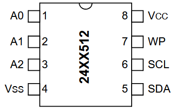
| Pin | Name | Description | Pin | Name | Description | |
|---|---|---|---|---|---|---|
| 1 | A0 | Address select pin 0* | 8 | VCC | Power supply | |
| 2 | A1 | Address select pin 1* | 7 | WP | Write protect* | |
| 3 | A2 | Address select pin 2* | 6 | SCL | I2C Clock line | |
| 4 | GND | Ground | 5 | SDA | I2C Data line |
Address select pins
These pins are optional, and may not be present on all chips. If they are present, they are used to select the I2C address of the chip. The address is 7 bits, with the last bit being the read/write bit. The address is determined by the state of these pins, e.g. A0=0, A1=0, A2=0 gives 7-bit address 0x50, A0=1, A1=0, A2=0 gives address 0x51, etc.
Write protect pin
The write protect pin is also optional, and may not be present on all chips. If it is present, it is used to protect the chip from being written to. If the pin is connected to ground, the chip can be written to. If the pin is connected to VCC, the chip is write protected and cannot be written to.
Image source: Microchip 24x512 datasheet
I2C EEPROM voltage requirements
| 24xx Family | Minimum Voltage | Maximum Voltage | Notes |
|---|---|---|---|
| AT24C | 2.7V | 5.5V | 400kHz max |
| 24C | 2.7V | 5.5V | 400kHz max |
| 24LC | 2.5V | 5.5V | 400kHz max |
| 24AA | 1.7V | 5.5V | 400kHz max |
| 24FC | 1.8V | 5.5V | 1MHz max |
3.3 volts is a good voltage to use with most 24x chips, but a few newer chips may have a lower maximum voltage. Always check the datasheet for the specific chip you are using if possible.
Identifying 1-Wire EEPROM chips
1-Wire EEPROMs are slightly different than SPI and I2C EEPROMs. Writes must be a full page (8 or 32 bytes) at a time, and they have much lower write cycles and data retention than SPI or I2C EEPROMs.
- Write: A full page (8 or 32 bytes), write aligned to the page size.
- Write cycles: 200,000
- Data retention: 10-25 years
1-Wire EEPROM chips are usually labeled with a part number starting with “243”. The “243” series includes chips like DS2431, DS2432, GX2341, DS24B33, etc. The “243” series is the only known series of 1-Wire EEPROMs.
The eeprom command in 1-Wire mode can probe, read, write, erase, verify and test most 1-Wire EEPROM chips.
| Device | Size | Bytes | Page Size | Addr Bytes | Blk Sel Bits | kHz max |
|---|---|---|---|---|---|---|
| DS2431** | 1K | 128 | 8 | 2 | 0 | 16 |
| DS24B33** | 4K | 512 | 32 | 2 | 0 | 16 |
**Tested devices
There are only two widely used 1-Wire EEPROM: DS2431+ (1Kbit) and DS24B33 (4Kbit). There is also a clone of the DS2431+ called GX2431.
1-Wire EEPROM voltage requirements
| Family | Minimum Voltage | Maximum Voltage | |
|---|---|---|---|
| DS243X | 2.8V | 5.25V |
This device family is so small, use 3.3 volts or 5 volts and you should be fine.
Identifying Microwire EEPROM chips
Microwire EEPROM chips are ancient technology that persists today. Microwire EEPROMs are also byte-addressable and can be written to one byte at a time. They use a funky version of SPI and have a drastically different pinout.
Microwire EEPROM chips are usually labeled with a part number starting with “93”. The “93” series includes chips like 93C46A, 93C56B, 93C66C, etc.
93x is available with 8 bit or 16 bit addressing.
- In 8 bit mode the memory appears as an array of 8 bit bytes. Each write operation writes one 8 bit byte.
- In 16 bit mode the memory appears as an array of 16 bit words. Each write operation writes two 8 bit bytes.
“A” part numbers are 8 bit, “B” part numbers are 16 bit. “C” part numbers can be either, depending on the state of the ORG pin.
The eeprom command in SPI mode can probe, read, write, erase, verify and test most Microwire EEPROM chips.
| Device | Size | Bytes | Organization | Dummy bits | Address | Total bits |
|---|---|---|---|---|---|---|
| 93x46A** | 1Kbit | 128 | x8 only | 0 | 7bits | 10 |
| 93x46B** | 1Kbit | 128 | x16 only | 0 | 6bits | 9 |
| 93x46C/E** | 1Kbit | 128 | x8 or x16 | 0 | 7 or 6bits | 10 or 9 |
| 93x56A** | 2Kbit | 256 | x8 only | 1 | 8bits | 12 |
| 93x56B** | 2Kbit | 256 | x16 only | 1 | 7bits | 11 |
| 93x56C** | 2Kbit | 256 | x8 or x16 | 1 | 8 or 7bits | 12 or 11 |
| 93x66A** | 4Kbit | 512 | x8 only | 0 | 9bits | 12 |
| 93x66B** | 4Kbit | 512 | x16 only | 0 | 8bits | 11 |
| 93x66C** | 4Kbit | 512 | x8 or x16 | 0 | 10 or 9bits | 12 or 11 |
| 93x76A | 8Kbit | 1024 | x8 only | 1 | 10bits | 14 |
| 93x76B | 8Kbit | 1024 | x16 only | 1 | 9bits | 13 |
| 93x76-/C | 8Kbit | 1024 | x8 or x16 | 1 | 10 or 9bits | 14 or 13 |
| 93x86A** | 16Kbit | 2048 | x8 only | 0 | 11bits | 14 |
| 93x86B** | 16Kbit | 2048 | x16 only | 0 | 10bits | 13 |
| 93x86-/C** | 16Kbit | 2048 | x8 or x16 | 0 | 11 or 10bits | 14 or 13 |
**Tested devices
For “C” devices, x8 or x16 bits is selected by the ORG pin. If ORG is low, the device is x8, if ORG is high, the device is x16.
Microwire EEPROM pinout
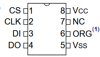
| Pin | Name | Description | Pin | Name | Description | |
|---|---|---|---|---|---|---|
| 1 | CS | SPI Chip Select (active HIGH) | 8 | VCC | Power supply | |
| 2 | CLK | SPI Clock | 7 | NC | Not Connected | |
| 3 | DI | SPI Data In (MOSI) | 6 | ORG | Address mode* | |
| 4 | DO | SPI Data Out (MISO) | 5 | GND | Ground |
Chip Select pin
The chip select pin is active high, which is different than most SPI devices.
ORG pin
The ORG pin is used to select the addressing mode of the chip. It is only present on “C” part numbers.
- LOW/GROUND: 8-bit addressing
- HIGH/VCC: 16-bit addressing
To determine the addressing mode of a “C” part number, you can measure the ORG pin with a multimeter. If it is connected to ground, the chip is in 8-bit mode. If it is connected to VCC, the chip is in 16-bit mode.
Image source: Microchip 93xx46 datasheet
Microwire EEPROM voltage requirements
| Family | Minimum Voltage | Maximum Voltage |
|---|---|---|
| 93C | 4.5V | 5.5V |
| M93C | 2.5V | 5.5V |
| 93LC | 2.5V | 5.5V |
| 93AA | 1.8V | 5.5V |
| AT93C | 2.7V | 5.5V |
93x chips are quite old, it is generally safe to use 5 volts with all versions. However, some newer chips may have a lower maximum voltage. Always check the datasheet for the specific chip you are using if possible.
FRAM Memory
SPI FRAM chips are a type of non-volatile memory that uses ferroelectric RAM technology. They are faster than EEPROM and Flash. FRAM can be written one byte at a time, or continuously without stop. FRAM has a very high write endurance and can be used in applications that require frequent writes.
- Size: 1Kbit to 4 Mbit (128B - 512K)
- Read: Byte addressable, can read any byte in the chip.
- Write: Continuous write, can write any byte in the chip. No concept of pages or sectors.
- Erase: No separate erase process is needed, bytes are erased individually before writing.
- Cost: FRAM is the most expensive memory in wide spread use, but is becoming more affordable.
- Write cycles: 10^15+ (1,000,000 times more than EEPROM)
- Data retention: 100+ years
Identifying SPI FRAM chips
SPI FRAM chips are usually labeled with a part number starting with “FM25” or “MB85”. The “FM25” series includes chips like FM25CL64B, FM25L04B, etc. The MB85RS series is Infineon’s name for their FRAM chips, e.g. MB85RS512.
The eprom command in SPI mode can probe, read, write, erase, verify and test most SPI FRAM chips. Choose a 25x EEPROM device with the same size as the FRAM chip you are using, e.g. if you have a 1Mbit FRAM chip, use 25x1024.
Identifying I2C FRAM chips
I2C FRAM chips are usually labeled with a part number starting with “FM24” or “MB85”. The “FM24” series includes chips like FM24CL64B, FM24L04B, etc. The MB85RC series is Infineon’s name for their FRAM chips, e.g. MB85RC64.
The eprom command in I2C mode can probe, read, write, erase, verify and test most I2C FRAM chips. Choose a 24x EEPROM device with the same size as the FRAM chip you are using, e.g. if you have a 32Kbit FRAM chip, use 24x32.
FRAM voltage requirements
| Family | Minimum Voltage | Maximum Voltage |
|---|---|---|
| FM25 | 2.7V | 3.65 |
| FM24 | 2.7V | 3.65 |
| MB85 | 2.7V | 3.6V |
FRAM chips are new and generally tolerate no more than 3.3V. Always check the datasheet for the specific chip you are using if possible.