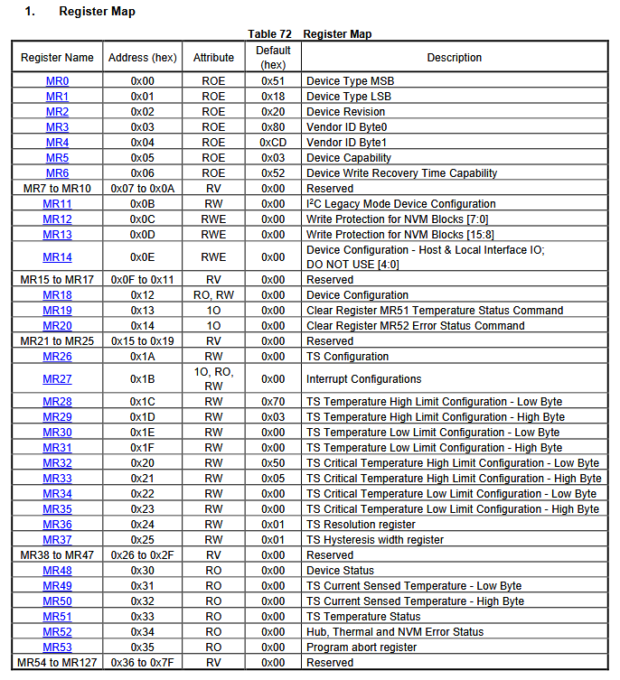
DDR5 SDRAM module I2C
DDR SDRAM modules are the memory sticks used in computers and laptops. DDR modules have a small EEPROM chip programmed with Serial Presence Detect (SPD) data. Motherboards use SPD data to configure DDR RAM and optimize performance.
DDR5 is the current latest DDR RAM standard. It has a much more complex SPD system than previous DDR versions, with integrated temperature monitoring and power management. We can use the Bus Pirate to learn about the DDR5 SPD system, and rescue modules with corrupted SPD data.
If you only want to backup or restore the SPD data without all the technical details, skip to the ddr5 command.
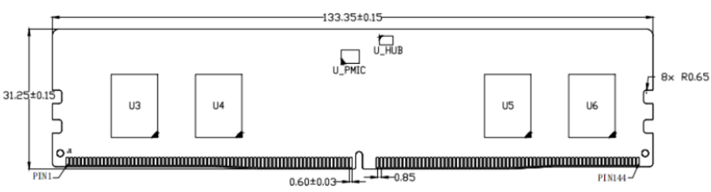
DDR1 to DDR4 modules had a simple I2C EEPROM chip that stored configuration information used by the motherboard. Aside from a little storage, the modules were pretty dumb. DDR5 has several new components that make it a much smarter, more active device.
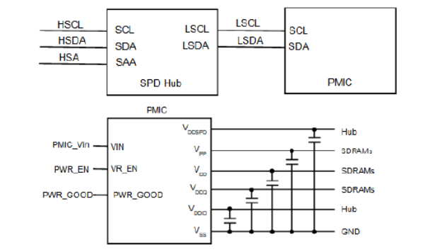
The SPD hub chip (U_HUB) has 1024 bytes of EEPROM memory to store configuration settings, but it also does much more.
- 1024 bytes of non-volatile memory for storing SPD data
- Temperature sensor with 4 levels of temperature alarms and error management features
- Configures the PMIC (Power Management IC) that supplies power to the memory chips
- I2C interface for reading and writing the SPD data
The PMIC (U_PMIC) is a sophisticated onboard power supply system for the RAM chips. In previous versions of DDR RAM the motherboard supplied all the voltages the memory chips need. The PMIC uses a single 5 volt supply to produce all the other voltages the memory chips use. The PMIC has much more control over the RAM power supply and quality, which decreases the effect of motherboard power supply noise on the memory chips. The PMIC also has an I2C interface.
Image source: UniIC SCA08GU04M1F1C-48B UDIMM datasheet
Resources
This demo was made possible by several resources:
- UniIC SCA08GU04M1F1C-48B UDIMM and SCA32GS13M1F1C-48B SODIMM for DDR5 module pinout and connections
- ABLIC S-34HTS08AB for the SPD hub interface and registers
- JEDEC JESD400-5C for the SPD hub non-volatile memory organization and contents
- Richtek RTQ5119A for PMIC interface and registers
Warning and Disclaimer
Follow this guide at your own risk. Don’t experiment with expensive high capacity, high speed, overclocker-special DDR5. We picked up cheap 8GB sticks from an e-Waste recycler, and we don’t care if they get damaged.
THE SOFTWARE, HARDWARE, AND TUTORIAL ARE PROVIDED “AS IS”, WITHOUT WARRANTY OF ANY KIND, EXPRESS OR IMPLIED, INCLUDING BUT NOT LIMITED TO THE WARRANTIES OF MERCHANTABILITY, FITNESS FOR A PARTICULAR PURPOSE AND NONINFRINGEMENT. IN NO EVENT SHALL THE AUTHORS OR COPYRIGHT HOLDERS BE LIABLE FOR ANY CLAIM, DAMAGES OR OTHER LIABILITY, WHETHER IN AN ACTION OF CONTRACT, TORT OR OTHERWISE, ARISING FROM, OUT OF OR IN CONNECTION WITH THE SOFTWARE, HARDWARE, AND TUTORIAL OR THE USE OR OTHER DEALINGS IN THE SOFTWARE, HARDWARE, AND TUTORIAL.
Connections
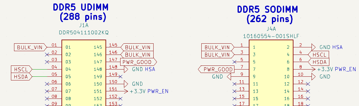
| DDR5 UDIMM (288 pins) | DDR5 SODIMM (262 pins) | Description |
|---|---|---|
| HSDA (5) | HSDA (6) | I2C Data (3.3volt) must be level shifted |
| HSCL (4) | HSCL (4) | I2C Clock (3.3volt) must be level shifted |
| PWR_EN(151) | PWR_EN (8) | Power Enable, connect to 3.3 volts |
| HSA (148) | HSA (2) | Host Sideband Address, connect to ground for address 0 (Offline Mode) |
| PWR_GOOD (147) | PWR_GOOD (7) | Power Good, optional (low for error) |
| BULK_VIN (3) | BULK_VIN (1) | Bulk Voltage Input, connect to 5 volts |
| GND (150) | GND(9) | Ground |
We only need to connect a few pins to access the SPD hub on a DDR5 module. The rest of the pins are used for power, data, and control signals.
- HSDA and HSCL are the I2C data and clock pins. While the DDR5 module is powered by 5 volts, the I2C pins must be no more than 3.3 volts. Use a level shifter to connect these pins if needed.
- HSA sets the SPD and PMIC I2C address. Motherboards accept multiple DDR5 modules, so each module needs a unique I2C address. A pull-down resistor connected to the HSA pin sets the last four bits of the base I2C address (0x50). When HSA is connected to ground the module goes into a special offline service mode that allows us to change write protected portions of the EEPROM.
- PWR_EN enables the DDR5 module power supply when connected to 3.3 volts.
- PWR_GOOD is an open drain output signal from the PMIC. If the power is stable this pin will float, but if the supply is interrupted it will pull low. This might be useful for diagnosing a faulty DDR5 module power supply.
- BULK_VIN is the single 5 volt power supply for the SDP hub and PMIC. There are multiple BULK_VIN pins on a DDR5 module, but only one needs to be connected to access the SPD hub.
- GND is the ground pin. There are multiple GND pins on a DDR5 module, but only one needs to be connected to access the SPD hub.
There are multiple BULK_VIN and GND pins on a DDR5 module, but only one of each needs to be connected to access the SPD hub.
The DDR5 HSDA and HSCL pins must be no more than 3.3 volts, but the DDR5 module is powered by 5 volts!
Use the DDR5 plank which has a 3.3 volt regulator and level shifters for the I2C pins. The Bus Pirate VOUT should be 5 volts, the plank takes care of the rest.
Bus Pirate VOUT set to 3.3 volts, power I2C pins and BULK_VIN from the 3.3 volt VOUT supply. This seems to work but the PWR_GOOD indicator will show a power supply fault.
Bus Pirate VOUT at 3.3 volts to power the I2C pins, power BULK_VIN from an external 5 volt supply. Don’t forget to connect the common ground pins of each supply and the DDR5 module.
DDR5 adapter board
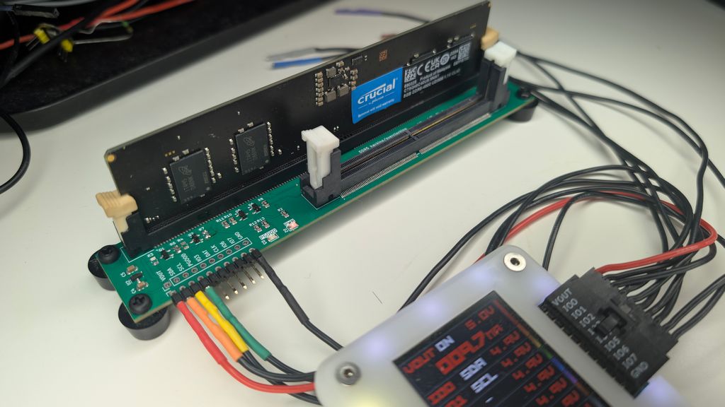
Soldering wires directly to a DDR5 module will probably render it unusable. Get a spare socket or adapter from your favorite supplier. Alternatively, the DDR5 adapter plank makes it easy to work with DDR5 UDIMM and SODIMM modules:
- 288 pin DDR5 UDIMM socket for standard desktop memory modules
- 262 pin DDR5 SODIMM socket for laptop memory modules
- Accepts a single 5 volt power supply
- A 3.3 volt regulator supplies the I2C and PWR_EN pins
- A level shifter ensures the I2C pins HSDA and HSCL are never more than 3.3 volts
- HSA is pulled to ground to put the module in offline mode
- PWR_GOOD is connected to an LED indicator that lights when the PMIC reports a voltage error
The DDR5 adapter plank is ready to use.
Get Bus Pirate & Accessories
Adapter Connections
| Bus Pirate | DDR5 adapter plank | Description |
|---|---|---|
| VOUT | BULK_VIN | 5 volt power supply for the DDR5 module |
| SDA (IO0) | HSDA | Level translated I2C Data |
| SCL (IO1) | HSCL | Level translated I2C Clock |
| GND | GND | Common ground for the DDR5 module and the Bus Pirate |
Connect the Bus Pirate to the DDR5 adapter plank as shown above. Four connection are all you need.
When inserting a DDR5 module into the adapter plank, hold the bottom of the PCB with both hands and press the module firmly into the socket. The retaining clips should click into place.
Be sure to adequately support the bottom of the PCB. Pressing without support will bend the PCB and break solder joints.
See it in action
Setup
HiZ> m i2c

Mode: I2C
I2C speed
 1kHz to 1000kHz
 x. Exit
kHz (400kHz*) > 400
Clock stretching
 1. OFF*
 2. ON
 x. Exit
OFF (1) > 1
I2C>
The DDR5 SPD hub uses the common and friendly I2C interface. Speeds of 100kHz, 400kHz, and 1MHz are supported.
Power supply
I2C> W 5
5.00V requested, closest value: 5.00V
300.0mA requested, closest value: 300.0mA

Power supply:Enabled
Vreg output: 5.0V, Vref/Vout pin: 5.0V, Current: 8.1mA

I2C>
DDR5 modules need a 5 volt BULK_VIN power supply, but remember that the I2C pins HSDA and HSCL must be no more than 3.3 volts. We’re using the DDR5 adapter plank which has a 3.3 volt regulator and level shifters for the I2C pins. The Bus Pirate VOUT should be 5 volts, the plank takes care of the rest.
W 5- enable the onboard power supply at 5 volts.
Refer to the power supply requirements above to avoid damaging your DDR5 module. The DDR5 module is powered by 5 volts, but the I2C pins HSDA and HSCL must be no more than 3.3 volts.
Pull-up resistors
I2C> P
Pull-up resistors: Enabled (10K ohms @ 5.0V)

I2C>
I2C is an open collector output bus, the Bus Pirate and the SPD chip can only pull the line low to 0 (ground). A pull-up resistor is needed to pull the line high to 1 (5 volts). The Bus Pirate has built-in pull-up resistors that can be enabled with the P command.
P- Enable the onboard pull-up resistors.
Be sure to enable the pull-up resistors. The data line will never go high without them and you’ll read only 0s.
I2C address scan
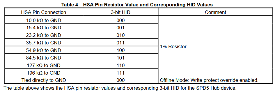
The DDR5 SPD hub has a base I2C address of 0x50. Bits 3 to 1 of the address are set by the HSA pin, which is pulled low to ground in this demo (0b000). This gives us a final I2C address of 0x50 (0xA0 write, 0xA1 read).
Image source: ABLIC S-34HTS08AB datasheet.
I2C> scan
I2C address search:
0x48 (0x90 W) (0x91 R)
0x50 (0xA0 W) (0xA1 R)
0x7E (0xFC W)

Found 5 addresses, 2 W/R pairs.

I2C>
Let’s see if we can find the I2C address with the I2C address scan.
scan- Scan the I2C bus for devices
The scanner found an I2C device at address 0x50 (0xA0 write, 0xA1 read). That’s the SPD hub chip. The second device at 0x48 (0x90 write, 0x91 read) is the PMIC (Power Management IC) that generates the vonltages for the DDR5 memory chips.
If the scanner doesn’t find the device, ensure the power supply is enabled W 5 and the pull-up resistors are enabled P.
SPD Hub Memory Areas
The SPD hub has two different memory areas:
- Registers - 128 bytes of registers that control the SPD hub and store things like the current temperature sensor reading.
- Non-Volatile Memory - 1024 byte EEPROM that stores JEDEC 5118 standard SPD data such as the memory size, speed, and timings.
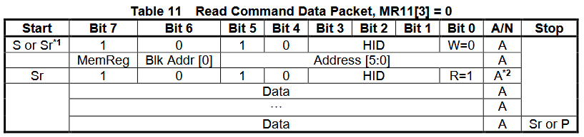
Accessing the SPD hub follows the common I2C pattern of setting the address pointer, then reading or writing data. Here’s the trick: the MemReg bit (bit 7) of the register address determines which memory area to access.
- 0b
0xxxxxxx - If MemReg is 0, the registers are accessed. The lower 7 bits select register byte 0-127. - 0b
1xxxxxxx - If MemReg is 1, the EEPROM/NVM is accessed. The lower 7 bits select byte 0-127 in the current NVM page (0-7).
Screenshots for the SPD hub IC sourced from ABLIC S-34HTS08AB datasheet.
SPD Hub Registers
Here’s a list of registers in the SPD hub. There’s 128 bytes total, but a lot of them are reserved for future use.
I2C> [0xa0 0b00000000 [ 0xa1 r:128]

I2C START
TX: 0xA0 ACK
TX: 0b00000000 ACK
I2C REPEATED START
TX: 0xA1 ACK
RX: 0x51 ACK 0x18 ACK 0x08 ACK 0x86 ACK 0x32 ACK 0x03 ACK 0x32 ACK 0x00 ACK
    0x00 ACK 0x00 ACK 0x00 ACK 0x00 ACK 0xFF ACK 0x03 ACK 0x00 ACK 0x00 ACK
    0x00 ACK 0x00 ACK 0x00 ACK 0x00 ACK 0x00 ACK 0x00 ACK 0x00 ACK 0x00 ACK
    0x00 ACK 0x00 ACK 0x00 ACK 0x00 ACK 0x70 ACK 0x03 ACK 0x00 ACK 0x00 ACK
    0x50 ACK 0x05 ACK 0x00 ACK 0x00 ACK 0x00 ACK 0x00 ACK 0x00 ACK 0x00 ACK
    0x00 ACK 0x00 ACK 0x00 ACK 0x00 ACK 0x00 ACK 0x00 ACK 0x00 ACK 0x00 ACK
    0x04 ACK 0x64 ACK 0x01 ACK 0x00 ACK 0x00 ACK 0x00 ACK 0x00 ACK 0x00 ACK
    0x00 ACK 0x00 ACK 0x00 ACK 0x00 ACK 0x00 ACK 0x00 ACK 0x00 ACK 0x00 ACK
    0x00 ACK 0x00 ACK 0x00 ACK 0x00 ACK 0x00 ACK 0x00 ACK 0x00 ACK 0x00 ACK
    0x00 ACK 0x00 ACK 0x00 ACK 0x00 ACK 0x00 ACK 0x00 ACK 0x00 ACK 0x00 ACK
    0x00 ACK 0x00 ACK 0x00 ACK 0x00 ACK 0x00 ACK 0x00 ACK 0x00 ACK 0x00 ACK
    0x00 ACK 0x00 ACK 0x00 ACK 0x00 ACK 0x00 ACK 0x00 ACK 0x00 ACK 0x00 ACK
    0x00 ACK 0x00 ACK 0x00 ACK 0x00 ACK 0x00 ACK 0x00 ACK 0x00 ACK 0x00 ACK
    0x00 ACK 0x00 ACK 0x00 ACK 0x00 ACK 0x00 ACK 0x00 ACK 0x00 ACK 0x00 ACK
    0x00 ACK 0x00 ACK 0x00 ACK 0x00 ACK 0x00 ACK 0x00 ACK 0x00 ACK 0x00 ACK
    0x00 ACK 0x00 ACK 0x00 ACK 0x00 ACK 0x00 ACK 0x00 ACK 0x00 ACK 0x00 NACK

I2C STOP
I2C>
We can dump all 128 bytes with a single I2C transaction. We’ll start reading at address 0, with MemReg set to 0 to access the registers. The write and read command must be separated by an I2C repeated start, the address pointer will reset to 0 after any STOP bit.
[- I2C START bit0xa0- I2C address and write bit0b00000000- Register address pointer, MemReg = 0, address 0,[- I2C Repeated START bit0xa1- I2C address and read bitr:128- Read 128 bytes]- I2C STOP bit
Let’s break it down and look at a few of the interesting registers.
Device Type
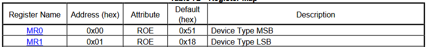
Register 0 and 1 contain the device type, 0x5118 for SPD5 hub with temperature sensor. The designers were being cute - 5118 is the JEDEC standard number for DDR5 SPD hubs.
I2C> [0xa0 0x00 [ 0xa1 r:2]

I2C START
TX: 0xA0 ACK 0x00 ACK
I2C REPEATED START
TX: 0xA1 ACK
RX: 0x51 ACK 0x18 NACK
I2C STOP
I2C>
Reading two bytes starting at register 0 (0x00) gives us the device type.
[ 0xa0 0x00 [ 0xa1 r:2 ]- Read the first two registers.
The device type is 0x5118, we have a DDR5 SPD hub with temperature sensor.
Temperature Sensor
Hang on tight! Reading the temperature is quite the ride, skip if you like.
- Read the temperature sensor resolution from register 36 (0x24).
- Read the temperature from register 49 and 50 (0x31, 0x32).
- Shift some bits around.
- Multiply by the resolution multiplier.
Temperature Sensor Resolution
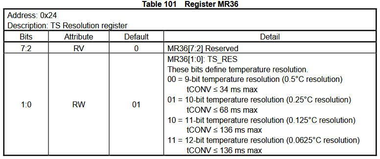
First we need to know the currently configured temperature sensor resolution. This is stored in register 36 (0x24).
I2C> [0xa0 0x24 [ 0xa1 r]

I2C START
TX: 0xA0 ACK 0x24 ACK
I2C REPEATED START
TX: 0xA1 ACK
RX: 0x00 NACK
I2C STOP
I2C>
[ 0xa0 0x24 [ 0xa1 r ]- Read the temperature sensor resolution from register 36 (0x24).
Register 36 is currently 0x00, so each bit of the temperature reading is 0.5 degrees Celsius.
Use the = convert format command to convert between number formats.
= 0x01= 0b01 (10-bit resolution, 0.25 celsius per bit)= 0x02= 0b10 (11-bit resolution, 0.125 celsius per bit)= 0x03= 0b11 (12-bit resolution, 0.0625 celsius per bit)
Change Temperature Sensor Resolution
Is your default resolution something other than 9 bits? Let’s change it to 9 bits so it matches this demo.
I2C> [0xa0 0x24 0b00]

I2C START
TX: 0xA0 ACK 0x24 ACK
TX: 0b00000000 ACK
I2C STOP
I2C>
Write 0b00 to register 36 (0x24) to set the temperature sensor resolution to 9 bits (0.5 degrees Celsius per bit).
[ 0xa0 0x24 0b00]- Write the temperature sensor resolution to register 36 (0x24).
You can repeat the previous step to verify the register is configured for 9 bits temperature sensing.
Read Temperature
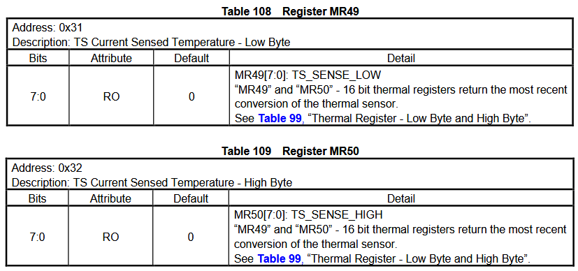
Registers 49 and 50 (0x31, 0x32) contain the current temperature sensor measurement.
I2C> [0xa0 0x31 [ 0xa1 r:2 ]

I2C START
TX: 0xA0 ACK 0x31 ACK
I2C REPEATED START
TX: 0xA1 ACK
RX: 0x54 ACK 0x01 NACK
I2C STOP
I2C>
[ 0xa0 0x31 [ 0xa1 r:2 ]- Read the temperature from registers 49 and 50 (0x31, 0x32).
The raw temperature sensor reading is 0x54 0x01. Now we need to shift the bits around and multiply by the resolution multiplier to get the actual temperature in degrees Celsius.
Calculate Temperature
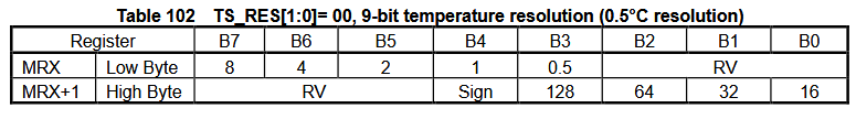
A 9 bit sensor measurement is packed into the two register bytes as shown in the table.
Let’s start with the low byte: 0x54 = 0b0101'0100.
- 0b
0101'0000 - Bits 7 to 3 are the low bits of the temperature measurement. - 0b0101'0
000- Bits 2 to 0 are discarded
The lower bits of the temperature are 0b01010. Now let’s do the high byte: 0x01 = 0b0000'0001.
- 0b
0000'0001 - Bits 7 to 5 are discarded. - 0b000
0‘0001 - Bit 4 is the sign bit, 0 for positive, 1 for negative. - 0b0000’
0001- Bits 3 to 0 are the high bits of the temperature measurement.
Put it all together:
- 0b
0'0010'1010 - The four bits from the high byte. - 0b0'001
0'1010- The five bits from the low byte.
Converting from binary to decimal gives us 0b0'0010'1010 = 42.
$$\text{Temp} = \left(\text{Multiplier} \times \text{value}\right)$$ $$\text{Temp} = \left(0.5 \times \text{value}\right)$$ $$\text{Temp} = \left(0.5 \times 42\right)$$ $$\text{Temp} = 21 \text{c}%$$
Multiply by the resolution multiplier of 0.5 degrees Celsius per bit to get 21 degrees Celsius. The sign bit is 0, so the temperature is a positive value.
EEPROM Block Protection Bits
The next three sections are SPD registers that control how the EEPROM/Non-Volatile Memory is configured.

The SPD EEPROM is made up of 16 block of 64 bytes each. Each block can be protected by setting the corresponding bit in register 12 and 13 from 0 to 1.
I2C> [0xa0 0x0c [ 0xa1 r:2 ]

I2C START
TX: 0xA0 ACK 0x0C ACK
I2C REPEATED START
TX: 0xA1 ACK
RX: 0xFF ACK 0x03 NACK
I2C STOP
I2C> = 0xff
 =0xFF =255 =0b11111111
I2C> = 0x03
 =0x03 =3 =0b00000011
I2C>
Read register 12 and 13 (0x0C, 0x0D) to see the current block protection configuration.
[ 0xa0 0x0c [ 0xa1 r:2 ]- Read the block protection bits from registers 12 and 13 (0x0C, 0x0D).
The JEDEC standard directs that manufacturers protect blocks 0 to 9, though some don’t lock 8 and 9.
- 0xFF = 0b1111'1111, blocks 7 to 0 are protected.
- 0x03 = 0b0000'0011, blocks 9 to 8 are protected.
To write protect additional blocks, set the corresponding bit in register 12 and 13 to 1. For example write 0xFF 0xFF to write protect all blocks. Don’t do this without first backing up the EEPROM!
It is always possible to protect new blocks, but write protection cannot be disabled (change 1 to 0) unless the module is in offline mode, with the HSA pin connected to ground.
Device Status Register
![]()
The Device Status register (48, 0x30) has two especially useful bits.
I2C> [0xa0 0x30 [ 0xa1 r]

I2C START
TX: 0xA0 ACK 0x30 ACK
I2C REPEATED START
TX: 0xA1 ACK
RX: 0x04 NACK
I2C STOP
I2C> = 0x04
 =0x04 =4 =0b00000100
I2C>
[0xa0 0x30 [ 0xa1 r ]- Read the device status from register 48 (0x30).
Device status is 0x04 = 0b0000'0100. Let’s decipher the bits with the datasheet.
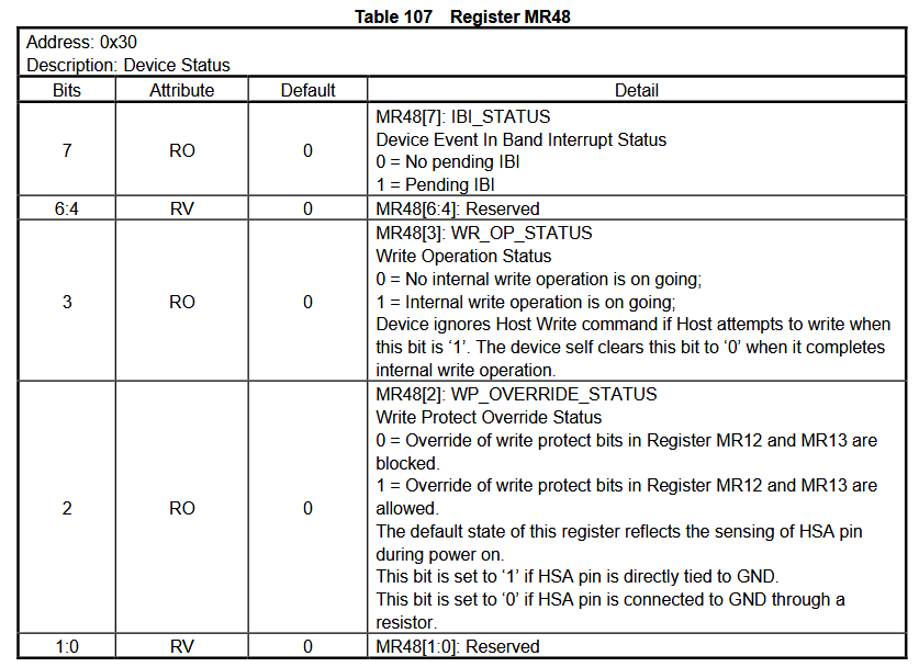
Bit 2 is set to 1, indicating the module is in offline mode. This means the HSA pin is connected to ground and we can remove write protection from the EEPROM blocks.
Bit 3 is set to 0, indicating that there is no write operation in progress. Writing to the EEPROM and updating the block protection registers take time, the SPD hub sets this bit to 1 while a write is in progress.
Legacy Mode and Page Setting
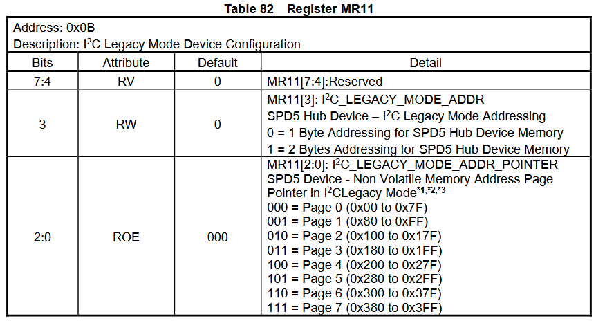
Our final stop on the tour of registers is the Legacy Mode Device Configuration register (11, 0x0B). Bit 3 controls how we select where to read and write in the EEPROM when the MemReg bit is high.
1 Byte Address Mode
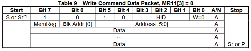
The EEPROM is divided into 8 pages of 128 bytes. In Legacy Mode (register 11 bit 3 = 0) when MemReg bit is 1:
- The lower seven bits select byte 0-127 in the EEPROM page (Blk_Addr[0] + Address[5:0]).
- Bits 2:0 in the Legacy Mode Device Configuration register select page 0-7.
Two transactions are needed to change between pages.
- A write to the Legacy Mode Device Configuration register to set the page.
- A write to the EEPROM with the MemReg bit set to 1 and the lower 7 bits set to the byte address within the page.
2 Byte Address Mode
The EEPROM is divided into 8 pages of 128 bytes. In 2 Byte Addressing mode (register 11 bit 3 = 1) when the MemReg bit is 1:
- The lower seven bits select bytes 0-127 in the EEPROM (Blk_Addr[0] + Address[5:0]).
- A second address byte selects page 0-7 (Blk_Addr[4:1]).
Non-Legacy Mode is easier to use because the page is selected with a second address byte. However, if the Legacy Mode configuration is wrong the second byte can be interpreted as data and will be accidentally written to the EEPROM. We’re going to stick with legacy mode for the added safety.
This description is only partly accurate. Technically when MemReg is 1 bit 6 is the first bit of the “block address” bits (Blk_Addr[0]), corresponding to the 16 write protect blocks of 64 bytes each. Functionally it can be treated as 7th address bit. This datasheet treats it both ways without actually addressing the inconsistency.
I2C> [0xa0 0x0b 0b00000000]

I2C START
TX: 0xA0 ACK 0x0B ACK
TX: 0b00000000 ACK
I2C STOP
I2C> [0xa0 0x0b [ 0xa1 r ]

I2C START
TX: 0xA0 ACK 0x0B ACK
I2C REPEATED START
TX: 0xA1 ACK
RX: 0x00 NACK
I2C STOP
I2C>
Legacy Mode addressing should be enabled by default, but let’s configure and verify it anyway.
[0xa0 0x0b 0b00000000]- Set the Legacy Mode Device Configuration register to 0, enabling legacy mode and setting the page to 0.[0xa0 0x0b [ 0xa1 r ]- Read the Legacy Mode Device Configuration register to verify it was set correctly.
Now we have the tools to read and write the SPD hub non-volatile memory.
Read SPD Hub Non-Volatile Memory
We’ve been through the swap of registers, now let’s see the show: the DDR5 SRAM settings stored in the SPD hub non-volatile memory. The content is defined by JEDEC standard JESD400-5C, free to download but registration required.
Normally we like to provide screenshots of actual datasheets to explain how devices work, but JEDEC is techy about sharing and watermarks each PDF. We’ll present a few simplified tables here instead of the normal screenshots.
Memory Organization
| Block | Range | Address Range | Description |
|---|---|---|---|
| 0-1 | 0-127 | 0x000-0x07F | Basic Information |
| 2 | 128-191 | 0x080-0x0BF | Reserved |
| 3-6 | 192-447 | 0x0C0-0x1BF | Module Parameters |
| 7 | 448-509 | 0x1C0-0x1FD | Reserved |
| 7 | 510-511 | 0x1FE-0x1FF | CRC for bytes 0-509 |
| 8-9 | 512-639 | 0x200-0x27F | Manufacturer Information |
| 10-15 | 640-1023 | 0x280-0x3FF | End User Programmable |
This is a simplified table of the SPD hub non-volatile memory organization.
Key Bytes
I2C> [0xa0 0x0b 0x00]

I2C START
TX: 0xA0 ACK 0x0B ACK 0x00 ACK
I2C STOP
I2C> [0xa0 0b10000000 [ 0xa1 r:4 ]

I2C START
TX: 0xA0 ACK
TX: 0b10000000 ACK
I2C REPEATED START
TX: 0xA1 ACK
RX: 0x30 ACK 0x10 ACK 0x12 ACK 0x02 NACK
I2C STOP
I2C>
The first four bytes are key to identifying a DDR5 module. First we need to set the Legacy Page address to 0, then the location to read inside page 0 with the MemReg bit set to 1.
[0xa0 0x0b 0x00]- Set Legacy Mode page pointer to page 0.[0xa0 0b10000000 [ 0xa1 r:4 ]- Read the first four bytes of the non-volatile memory, note the MemReg bit is set to 1.
Byte 2 (0x12) is the protocol type, which is always 0x12 for DDR5 modules. This indicates the module uses the DDR5 protocol.
Byte 3 (0x02 = 0b0000’0010) is the module type. The lower four bits indicate the type of module, 0b0010 is UDIMM and 0b0011 is SODIMM. There’s a large list of module types in JEDEC JESD400-5C, so be sure to check there if you’re working with something exotic.
| Bits 3:0 | Type |
|---|---|
| 0010 | UDIMM |
| 0011 | SODIMM |
The upper four bits of byte 3 are used to indicate hybrid module types, which we won’t cover here.
Byte 0 bits 4 to 6 (0x30 = 0b0011‘000) encode the EEPROM size. This should be 011 for DDR5 SDP5112, 1024 bytes total.
Byte 1 (0x10 = 0b0001'0000) encodes the SPD revision. The high four bits are the major revision, the low four bits are the minor revision. 0x10 is revision 1.0.
After the key bytes there is information about the SDRAM chips on the module: capacity, organization, speed, timings, etc. See the JEDEC JESD400-5C standard for all the juicy details.
Manufacturer Info
| Byte Number | Address | Description |
|---|---|---|
| 512-513 | 0x200-0x201 | Module Manufacturer JEDEC ID |
| 515-516 | 0x203-0x204 | Module Manufacturing Date |
| 517-520 | 0x205-0x208 | Module Serial Number |
| 521-550 | 0x209-0x226 | Module Part Number |
| 552-553 | 0x228-0x229 | DRAM Manufacturer ID |
| 555-637 | 0x22B-0x27D | Manufacturer Specific Data |
This is a simplified table of the manufacturer information stored in the SPD hub non-volatile memory. Only the most interesting fields are shown here.
The manufacturer information is stored in block 8 and 9, equivalent to page 4.
Module Manufacturer JEDEC ID
I2C> [0xa0 0x0b 0x04]

I2C START
TX: 0xA0 ACK 0x0B ACK 0x04 ACK
I2C STOP
I2C> [0xa0 0b10000000 [ 0xa1 r:2 ]

I2C START
TX: 0xA0 ACK
TX: 0b10000000 ACK
I2C REPEATED START
TX: 0xA1 ACK
RX: 0x85 ACK 0x9B NACK
I2C STOP
I2C>
First we need to set the Legacy Page address to 4, then we can read the manufacturer JEDEC ID from the non-volatile memory.
[0xa0 0x0b 0x04]- Set Legacy Mode page pointer to page 4.[0xa0 0b10000000 [ 0xa1 r:2 ]- Read the module manufacturer JEDEC ID at the beginning of the page.
0x859B is the JEDEC ID for Crucial Technology. JEDEC maintains a list, but it’s easier to find it with a web search.
Module Manufacture Date
I2C> [0xa0 0x83 [ 0xa1 r:2 ]

I2C START
TX: 0xA0 ACK 0x83 ACK
I2C REPEATED START
TX: 0xA1 ACK
RX: 0x22 ACK 0x04 NACK
I2C STOP
I2C>
Read the module manufacturing date from registers 515 and 516 (0x203, 0x204). The date is encoded as a year and week number.
[0xa0 0x0b 0x04]- Set Legacy Mode page pointer to page 4.[0xa0 0x83 [ 0xa1 r:2 ]- Read the module manufacturing date.
0x22 is the year, 0x04 is the week number. This module was manufactured in the 4th week of 2022.
At this stage we’ll stop writing the MemReg and address values in binary, and instead use hexadecimal. 0b10000000 = 0x80
Module Serial Number
I2C> [0xa0 0x85 [ 0xa1 r:4 ]

I2C START
TX: 0xA0 ACK 0x85 ACK
I2C REPEATED START
TX: 0xA1 ACK
RX: 0xE6 ACK 0xFF ACK 0xB7 ACK 0x85 NACK
I2C STOP
I2C>
Read the module serial number from registers 517 to 520 (0x205 to 0x208). The serial number is a 32-bit value.
[0xa0 0x0b 0x04]- Set Legacy Mode page pointer to page 4.[0xa0 0x85 [ 0xa1 r:4 ]- Read the module serial number.
0xE6FFB785 is the serial number, and it matches the serial printed on the module under the QR code.
Module Part Number
I2C> o

Number display format
 Current setting: Auto
 1. Auto
 2. HEX
 3. DEC
 4. BIN
 5. ASCII
 x. Exit
Mode > 5
Mode: ASCII
I2C>
The part number is a string of ASCII characters, so we’ll change the Bus Pirate output format to ASCII (type o, choose ASCII).
I2C> [0xa0 0x89 [ 0xa1 r:30 ]

I2C START
TX: 0xA0 ACK 0x89 ACK
I2C REPEATED START
TX: 0xA1 ACK
RX: 'C' 0x43 ACK 'T' 0x54 ACK '8' 0x38 ACK 'G' 0x47 ACK
    '4' 0x34 ACK '8' 0x38 ACK 'C' 0x43 ACK '4' 0x34 ACK
    '0' 0x30 ACK 'U' 0x55 ACK '5' 0x35 ACK '.' 0x2E ACK
    'M' 0x4D ACK '4' 0x34 ACK 'A' 0x41 ACK '1' 0x31 ACK
    ' ' 0x20 ACK ' ' 0x20 ACK ' ' 0x20 ACK ' ' 0x20 ACK
    ' ' 0x20 ACK ' ' 0x20 ACK ' ' 0x20 ACK ' ' 0x20 ACK
    ' ' 0x20 ACK ' ' 0x20 ACK ' ' 0x20 ACK ' ' 0x20 ACK
    ' ' 0x20 ACK ' ' 0x20 NACK
I2C STOP
I2C>
The part number is a 30 character ASCII text string starting at register 521 (0x209).
[0xa0 0x0b 0x04]- Set Legacy Mode page pointer to page 4.[0xa0 0x89 [ 0xa1 r:30 ]- Read the module part number.
The part number string is “CT8G48C40U5.M4A1”.
I2C> o

Number display format
 Current setting: ASCII
 1. Auto
 2. HEX
 3. DEC
 4. BIN
 5. ASCII
 x. Exit
Mode > 1
Mode: Auto
I2C>
Change the Bus Pirate output format back to AUTO before continuing (type o, choose AUTO).
DRAM Manufacturer JEDEC ID
I2C> [0xa0 0xa8 [ 0xa1 r:2 ]

I2C START
TX: 0xA0 ACK 0xA8 ACK
I2C REPEATED START
TX: 0xA1 ACK
RX: 0x80 ACK 0x2C NACK
I2C STOP
I2C>
There is a second JEDEC ID specifically to encode the DRAM chip manufacturer. We can grab this from registers 552 and 553 (0x228, 0x229).
[0xa0 0x0b 0x04]- Set Legacy Mode page pointer to page 4.[0xa0 0xa8 [ 0xa1 r:2 ]- Read the DRAM manufacturer JEDEC ID.
0x802C is the JEDEC ID for Micron Technology. Again, easiest to find with a web search.
Manufacturer Specific Data
I2C> [0xa0 0xab [ 0xa1 r:85 ]

I2C START
TX: 0xA0 ACK 0xAB ACK
I2C REPEATED START
TX: 0xA1 ACK
RX: 0x34 ACK 0x35 ACK 0x31 ACK 0x30 ACK 0x39 ACK 0x30 ACK 0x34 ACK 0x38 ACK
    0x31 ACK 0x39 ACK 0x00 ACK 0x00 ACK 0x00 ACK 0x00 ACK 0x00 ACK 0x00 ACK
    0x00 ACK 0x00 ACK 0x00 ACK 0x00 ACK 0x00 ACK 0x00 ACK 0x00 ACK 0x00 ACK
    0x00 ACK 0x00 ACK 0x00 ACK 0x00 ACK 0x00 ACK 0x00 ACK 0x00 ACK 0x00 ACK
    0x00 ACK 0x00 ACK 0x00 ACK 0x00 ACK 0x00 ACK 0x00 ACK 0x00 ACK 0x00 ACK
    0x00 ACK 0x00 ACK 0x00 ACK 0x00 ACK 0x00 ACK 0x00 ACK 0x00 ACK 0x00 ACK
    0x00 ACK 0x00 ACK 0x00 ACK 0x00 ACK 0x00 ACK 0x00 ACK 0x00 ACK 0x00 ACK
    0x00 ACK 0x00 ACK 0x00 ACK 0x00 ACK 0x00 ACK 0x00 ACK 0x00 ACK 0x00 ACK
    0x00 ACK 0x00 ACK 0x00 ACK 0x00 ACK 0x00 ACK 0x00 ACK 0x00 ACK 0x00 ACK
    0x00 ACK 0x00 ACK 0x00 ACK 0x00 ACK 0x00 ACK 0x00 ACK 0x00 ACK 0x00 ACK
    0x00 ACK 0x00 ACK 0x00 ACK 0x00 ACK 0x00 NACK
I2C STOP
I2C>
The last section is manufacturer specific data. This is a free area that can be used for anything the manufacturer wants, so it varies widely between manufacturers. It may contain additional overclocking profiles in EXPO (AMD) or XMP (Intel) format, it may also contain special keys that unscrupulous manufacturers use to lock a system to their specific brand of RAM module.
[0xa0 0x0b 0x04]- Set Legacy Mode page pointer to page 4.[0xa0 0xab [ 0xa1 r:85 ]- Read the manufacturer specific data from registers 555 to 637 (0x22B to 0x27D).
This module has a bit of extra data, but nothing special. It looks like it could be a short ASCII string “4510904819”.
Write SPD Hub Non-Volatile Memory
Writing to the SPD hub non-volatile memory is dangerous!
- It can make the module unbootable.
- It can make the module unusable.
Before writing to the SPD hub non-volatile memory, make sure you have a backup of the original data. Better yet, only experiment with a module you don’t care about.
We’re going to write a 16 byte page in the End User Programmable area of the SPD hub non-volatile memory, block 15. Despite the name, manufacturers do use this area to store overclocking profiles and other data. It is NOT safe to write in this area.
Unlock NVM Block Protection
I2C> [0xa0 0x0c 0xff 0x3f]

I2C START
TX: 0xA0 ACK 0x0C ACK 0xFF ACK 0x3F ACK
I2C STOP
I2C>
According to the JEDEC standard, the End User Programmable area is not write protected by default. Let’s update the EEPROM Block Protection Bits to make sure block 14 & 15 are not write protected.
[0xa0 0x0c 0xff 0x3f]- Write protect all blocks except block 14 & 15.
Writing 0xff (0b1111'1111) to register 12 (0x0C) write protects block 7-0. The next byte 0x7f (0b0011'1111) programs register 13 to protect blocks 8-13, while leaving blocks 14 & 15 unprotected.
Poll For Write Operation to Complete
I2C> [0xa0 0x30 [ 0xa1 r]

I2C START
TX: 0xA0 ACK 0x30 ACK
I2C REPEATED START
TX: 0xA1 ACK
RX: 0x04 NACK
I2C STOP
I2C> = 0x04
 =0x04 =4 =0b00000100
I2C>
Block protection is a persistent non-volatile setting that sticks even after power off. The SPD hub will take a few milliseconds to write the new block protection settings. We need to check in on our friend from earlier, the Device Status Register, to see when the write is complete.
[0xa0 0x30 [ 0xa1 r ]- Read the device status register to check if the write operation is complete.
Bit 3 is set to 0 (0x04 = 0b0000’0100), indicating the write operation is complete. The block protection bits are now set to protect all blocks except block 15.
Since we’re typing these commands manually, the write opertion is complete by the time we read the device status register. If you were writing a script or program to automate this, you would need to poll the device status register until bit 3 is 0.
Verify Write Protection Bits
I2C> [0xa0 0x0c [ 0xa1 r:2 ]

I2C START
TX: 0xA0 ACK 0x0C ACK
I2C REPEATED START
TX: 0xA1 ACK
RX: 0xFF ACK 0x3F NACK
I2C STOP
I2C>
Let’s verify the block protection bits are set correctly. We can read registers 12 and 13 (0x0C, 0x0D) to check the current block protection configuration.
[0xa0 0x0c [ 0xa1 r:2 ]- Read the block protection bits from registers 12 and 13 (0x0C, 0x0D).
Block protection bits are now 0xFF 0x7F, the update was successful.
If the Write Protection Bits are not correct, ensure that the module is in offline mode (HSA pin connected to ground) and check the Write Protect Override Status in the Device Status Register.
Read 16 Bytes
Writing to the SPD hub non-volatile memory is dangerous!
Before writing to the SPD hub non-volatile memory, make sure you have a backup of the original data. Better yet, only experiment with a module you don’t care about.
In this step we will read 16 bytes before writing to verify it is empty. If you see anything other than 0x00s then ABSOLUTLY DO NOT WRITE TO THAT LOCATION. It is likely that area is already programmed with some data, and writing to it will make the module unbootable or unusable.
I2C> [0xa0 0x0b 0x07]

I2C START
TX: 0xA0 ACK 0x0B ACK 0x07 ACK
I2C STOP
I2C> [0xa0 0b10000000 [ 0xa1 r:16 ]

I2C START
TX: 0xA0 ACK
TX: 0b10000000 ACK
I2C REPEATED START
TX: 0xA1 ACK
RX: 0x00 ACK 0x00 ACK 0x00 ACK 0x00 ACK 0x00 ACK 0x00 ACK 0x00 ACK 0x00 ACK
    0x00 ACK 0x00 ACK 0x00 ACK 0x00 ACK 0x00 ACK 0x00 ACK 0x00 ACK 0x00 NACK

I2C STOP
I2C>
First let’s read the target block to make sure it is empty. We’ll read the 16 bytes starting from byte 0 of block 14 (page 7).
[0xa0 0x0b 0x07]- Set Legacy Mode page pointer to page 7 (block 14 & 15).[0xa0 0b10000000 [ 0xa1 r:16 ]- Read 16 bytes from non-volatile memory.
Every byte should be 0x00 if the bytes are empty.
If you see anything other than 0x00s, then ABSOLUTELY DO NOT WRITE TO THAT LOCATION. It is likely that area is already programmed with some data, and writing to it will make the module unbootable or unusable.
Write 16 Bytes
I2C> [0xa0 0b10000000 0 1 2 3 4 5 6 7 8 9 10 11 12 13 14 15]

I2C START
TX: 0xA0 ACK
TX: 0b10000000 ACK
TX: 0 ACK 1 ACK 2 ACK 3 ACK 4 ACK 5 ACK 6 ACK 7 ACK
    8 ACK 9 ACK 10 ACK 11 ACK 12 ACK 13 ACK 14 ACK 15 ACK

I2C STOP
I2C>
The EEPROM is written 16 bytes at a time. Each write page must also be aligned to a 16 byte boundary, so the address of the first byte of the write page must be 0, 16, 32, etc. We’ll write 16 bytes of data to the non-volatile memory beginning at byte 0 of block 14.
[0xa0 0x0b 0x07]- Set Legacy Mode page pointer to page 7 (block 14 & 15).[0xa0 0b10000000 0 1 2 3 4 5 6 7 8 9 10 11 12 13 14 15]- Write 16 bytes.
If you were writing a script or program to automate this, you would need to poll the Device Status Register until bit 3 is 0 to ensure the write operation is complete. We’re moving slow enough that the write is complete by the next step.
Verify 16 Bytes
I2C> [0xa0 0b10000000 [ 0xa1 r:16 ]

I2C START
TX: 0xA0 ACK
TX: 0b10000000 ACK
I2C REPEATED START
TX: 0xA1 ACK
RX: 0x00 ACK 0x01 ACK 0x02 ACK 0x03 ACK 0x04 ACK 0x05 ACK 0x06 ACK 0x07 ACK
    0x08 ACK 0x09 ACK 0x0A ACK 0x0B ACK 0x0C ACK 0x0D ACK 0x0E ACK 0x0F NACK

I2C STOP
I2C>
Finally! let’s read back the 16 byte page we just wrote to verify it was written correctly.
[0xa0 0x0b 0x07]- Set Legacy Mode page pointer to page 7 (block 14 & 15).[0xa0 0b10000000 [ 0xa1 r:16 ]- Read the 16 byte page from the non-volatile memory.
The read data should match the data we wrote: 0 1 2 3 4 5 6 7 8 9 10 11 12 13 14 15.
Power management IC
Remember the second set of I2C addresses we found in the I2C address scan? The second device is the power management IC (PMIC) that generates voltages used by the SRAM chips.
The SPD hub is a hub because it contains the JEDEC SPD data for using the module, configures the PMIC and passes data through to the PMIC.
The PWR_EN and PWR_GOOD pin on the DDR5 module are actually connected to pins on the PMIC. PWR_GOOD is called CAMP (Control And Monitor Port), an open drain output. PWR_GOOD/CAMP is an input when the voltage is normal, and pulls low when the voltage is out of range.
On complex DDR5 modules, like DDR5 RDIMMs for servers, there are even more chips that are controlled by the SPD hub.
Screenshots for the PMIC sourced from Richtek RTQ5119A datasheet.
PMIC Memory Areas
There doesn’t really apear to anything super interesting in the PMIC registers to poke at. It’s mostly used by the SPD hub to configure PMIC voltage and current levels, power sequencing, and other power management features.
The DIMM Vendor area has a region password protected by a 16 bit password that seems ripe for a fun brute force attack. Not sure to what end though.
Dump PMIC Registers
I2C> [0x90 0x00 [0x91 r:64]

I2C START
TX: 0x90 ACK 0x00 ACK
I2C REPEATED START
TX: 0x91 ACK
RX: 0x00 ACK 0x00 ACK 0x00 ACK 0x00 ACK 0x00 ACK 0x00 ACK 0x00 ACK 0x00 ACK
    0x00 ACK 0x00 ACK 0x02 ACK 0x00 ACK 0x00 ACK 0x00 ACK 0x00 ACK 0x00 ACK
    0x00 ACK 0x00 ACK 0x00 ACK 0x00 ACK 0x00 ACK 0x2C ACK 0x20 ACK 0x00 ACK
    0x00 ACK 0x04 ACK 0x00 ACK 0x05 ACK 0x60 ACK 0x00 ACK 0x60 ACK 0x60 ACK
    0x89 ACK 0x78 ACK 0x63 ACK 0x00 ACK 0x00 ACK 0x78 ACK 0x67 ACK 0x78 ACK
    0x63 ACK 0x90 ACK 0x9A ACK 0x42 ACK 0x20 ACK 0x22 ACK 0x04 ACK 0x5A ACK
    0x00 ACK 0x00 ACK 0x80 ACK 0x04 ACK 0x0E ACK 0x00 ACK 0x00 ACK 0x00 ACK
    0x00 ACK 0x00 ACK 0x00 ACK 0x12 ACK 0x8A ACK 0x8C ACK 0x00 ACK 0x00 NACK

I2C STOP
I2C>
We can dump the PMIC registers just like we did with the SPD hub registers. The PMIC appears to have 256 bytes of registers, but let’s just dump the first 64.
[ 0x90 0x00 [ 0x91 r:64 ]- Read the first 64 bytes of PMIC registers from byte 0.
You can see that there’s something in there. Most of the higher addresses have limited access and seem to return 0x00 without some kind of additional configuration.
PMIC JEDEC Vendor ID
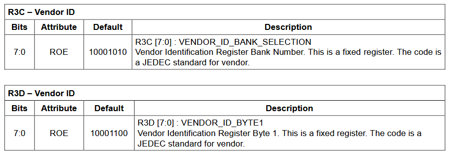
This PMIC datasheet shows a JEDEC ID at register 0x3C and 0x3D.
PMIC registers are also defined by a JEDEC standard, but you can get a free and friendly version in the datasheet for the Richtek RTQ5119A.
I2C> [0x90 0x3c [0x91 r:2]

I2C START
TX: 0x90 ACK 0x3C ACK
I2C REPEATED START
TX: 0x91 ACK
RX: 0x8A ACK 0x8C NACK
I2C STOP
I2C>
Let’s grab the JEDEC ID from registers 0x3C and 0x3D.
[0xa0 0x3c [ 0xa1 r:2 ]- Read the PMIC JEDEC vendor ID from registers 0x3C and 0x3D.
In a stunning coincidence, the JEDEC ID is 0x8A8C, which matches the Richtek RTQ5119A PMIC datasheet in the screenshot above.
ddr5 Command
All of this demo and more is automated by the ddr5 command. It can read, write, verify, dump, lock and unlock the SPD hub non-volatile memory, decode the registers and even read the temperature sensor. Learn about the ddr5 command in the command reference.
Get a Bus Pirate
Get Bus Pirate & Accessories
- Browse Complete Bus Pirate hardware collection
- Bus Pirate 5 REV10 with enclosure
- Probe Cable Kit
- Auxiliary Cable Kit
- Quick Connect Adapter