DDR4 SDRAM module I2C
This page is a work in progress. Some details may be missing or incomplete.
DDR4 is an older computer memory RAM standard. Each stick has a simple EEPROM that stores Serial Presence Detect (SPD) data. Motherboards use SPD data to configure DDR RAM and optimize performance. We can use the Bus Pirate to learn about the DDR4 stick, and rescue modules with corrupted SPD data.
If you only want to backup or restore the SPD data without all the technical details, skip to the ddr4 command.
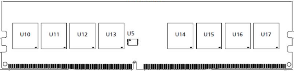
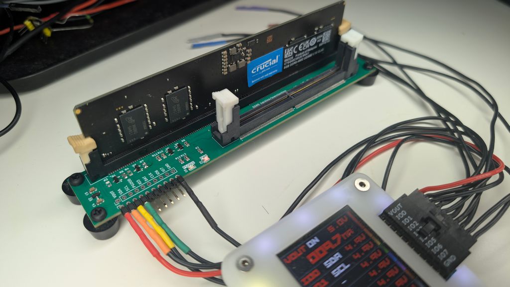
The DDR4 SPD EEPROM is the small chip labeled U5 on the module above. It is connected to an I2C bus, which we can access with the Bus Pirate.
Image source: UniIC SCC08GU03C2F1C-32AA UDIMM datasheet.
Resources
This demo was made possible by several resources:
- UniIC SCC08GU03C2F1C-32AA UDIMM and SCC04GS04H3F1C-32AA SODIMM for DDR4 module pinout and connections
- OnSemi N34C04 for the DDR4 SPD EEPROM interface
- JEDEC JESD21-C Annex L for the SPD organization and contents
Warning and Disclaimer
Follow this guide at your own risk. Don’t experiment with expensive high capacity, high speed, overclocker-special DDR4. We picked up cheap 4GB sticks from an e-Waste recycler, and we don’t care if they get damaged.
THE SOFTWARE, HARDWARE, AND TUTORIAL ARE PROVIDED “AS IS”, WITHOUT WARRANTY OF ANY KIND, EXPRESS OR IMPLIED, INCLUDING BUT NOT LIMITED TO THE WARRANTIES OF MERCHANTABILITY, FITNESS FOR A PARTICULAR PURPOSE AND NONINFRINGEMENT. IN NO EVENT SHALL THE AUTHORS OR COPYRIGHT HOLDERS BE LIABLE FOR ANY CLAIM, DAMAGES OR OTHER LIABILITY, WHETHER IN AN ACTION OF CONTRACT, TORT OR OTHERWISE, ARISING FROM, OUT OF OR IN CONNECTION WITH THE SOFTWARE, HARDWARE, AND TUTORIAL OR THE USE OR OTHER DEALINGS IN THE SOFTWARE, HARDWARE, AND TUTORIAL.
Connections
| DDR4 UDIMM (288 pins) | DDR4 SODIMM (260 pins) | Description |
|---|---|---|
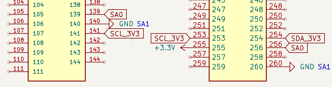
| SDA (5) | SDA (6) | I2C Data (3.3volt) must be level shifted |
| SCL (141) | SCL (4) | I2C Clock (3.3volt) must be level shifted |
| SA0 (139) | SA0 (256) | SPD I2C Address Bit 0, connect to ground for address 0, 9volts when changing write protection |
| SA1 (140) | SA1 (260) | SPD I2C Address Bit 1, connect to ground for address 0 |
| SA2 (238) | SA2 (166) | SPD I2C Address Bit 2, connect to ground for address 0 |
| VDD (284) | VDD (255) | 3.3 Volt Power Supply |
| VSS (2) | VSS (1) | Ground |
We need to connect to the EEPROM I2C pins, as well as set the default I2C address using the SA0, SA1, and SA2 pins. Finally, we need to provide power to the module.
- SDA and SCL are the I2C data and clock pins. The I2C pins must be no more than 3.3 volts.
- SA0 sets the least significant bit of the I2C address. Connect to ground for address 0 (0x50). To change the write protection settings, SA0 must be connected to 9 volts.
- SA1 and SA2 set the other bits of the I2C address. Connect both to ground for address 0 (0x50).
- VDD requires a 3.3 volt power supply. There are multiple VDD pins, but only one needs to be connected.
- VSS is the ground pin. There are multiple GND pins on a DDR4 module, but only one needs to be connected to access the SPD EEPROM.
There are multiple VDD and VSS pins on a DDR4 module, but only one of each needs to be connected to access the SPD EEPROM.
DDR4 adapter board
Soldering wires directly to a DDR4 module will probably render it unusable. Get a spare socket or adapter from your favorite supplier. Alternatively, the DDR4 adapter plank makes it easy to work with DDR4 UDIMM and SODIMM modules:
- 288 pin DDR4 UDIMM socket for standard desktop memory modules
- 260 pin DDR4 SODIMM socket for laptop memory modules
- 3.3 volt to 5 volt power supply
- A 3.3 volt regulator ensures the DDR4 module VDD pin is never more than 3.3 volts
- A level shifter ensures the I2C pins SDA and SCL are never more than 3.3 volts
- SA1 and SA2 are pulled to ground to set the I2C address to 0x50
- SA0 is normally ground, an optocoupler can connect it to 9 volts to change the write protection settings
- External 9 volt power supply required (typically a 9 volt battery)
The DDR4 adapter plank is ready to use, but you’ll need a 9 volt battery or bench supply.
Get Bus Pirate & Accessories
Adapter Connections
| Bus Pirate | DDR4 adapter plank | Description |
|---|---|---|
| VOUT | VOUT | 3.3 - 5 volt power supply for the DDR4 module |
| SDA (IO0) | SDA | Level translated I2C Data |
| SCL (IO1) | SCL | Level translated I2C Clock |
| SA0 (IO2) | SA0 | SPD I2C Address Bit 0, high enables the 9 volt supply to SA0 |
| HV_FB (IO3) | HV_FB | 9 volt power supply feedback, divided by three |
| GND | GND | Common ground for the DDR module and the Bus Pirate |
Connect the Bus Pirate to the DDR4 adapter plank as shown above. Four connection are all you need.
When inserting a DDR4 module into the adapter plank, hold the bottom of the PCB with both hands and press the module firmly into the socket. The retaining clips should click into place.
Be sure to adequately support the bottom of the PCB. Pressing without support will bend the PCB and break solder joints.
See it in action
Setup
HiZ> m i2c

Mode: I2C
I2C speed
 1kHz to 1000kHz
 x. Exit
kHz (400kHz*) > 100
Clock stretching
 1. OFF*
 2. ON
 x. Exit
OFF (1) > 1
I2C>
The DDR4 SPD EEPROM uses the common I2C protocol. Speeds of 100kHz, 400kHz, and 1MHz are supported.
Power supply
I2C> W 3.3
3.30V requested, closest value: 3.30V
300.0mA requested, closest value: 300.0mA

Power supply:Enabled
Vreg output: 3.3V, Vref/Vout pin: 3.3V, Current: 5.4mA

I2C>
DDR4 modules need a 3.3 volt power supply.
W 3.3- enable the onboard power supply at 3.3 volts.
To change write protection setting, you’ll also need an external 9 volt power supply that can be connected to SA0 when needed.
Pull-up resistors
I2C> P
Pull-up resistors: Enabled (10K ohms @ 3.3V)

I2C>
I2C is an open collector output bus, the Bus Pirate and the SPD EEPROM can only pull the line low to 0 (ground). A pull-up resistor is needed to pull the line high to 1 (3.3 volts). The Bus Pirate has built-in pull-up resistors that can be enabled with the P command.
P- Enable the onboard pull-up resistors.
Be sure to enable the pull-up resistors. The data line will never go high without them and you’ll read only 0s.
I2C address scan
The DDR4 SPD EEPROM has a base I2C address of 0x50. Bits 3 to 1 of the address are set by the SA2, SA1 and SA0 pins. We’ve pulled these pins to ground (0b000). This gives us a final I2C address of 0x50 (0xA0 write, 0xA1 read).
Image source: OnSemi N34C04 datasheet.
I2C> scan
I2C address search:
0x30 (0x61 R)
0x35 (0x6B R)
0x36 (0x6C W) (0x6D R)
0x37 (0x6E W)
0x50 (0xA0 W) (0xA1 R)

Found 7 addresses, 2 W/R pairs.

I2C>
Let’s see if we can find the I2C address with the I2C address scan.
scan- Scan the I2C bus for devices
We found a whole bunch of addresses, but we’ll get to that in a moment. The important address is 0x50, where we access the EEPROM data.
If the scanner doesn’t find the device, ensure the power supply is enabled W 3.3 and the pull-up resistors are enabled P.
Read SPD EEPROM
| Block | Range | Hex Range | Description |
|---|---|---|---|
| 0 | 0-127 | 0x000-0x07F | Base Configuration and DRAM Parameters |
| 1 | 128-191 | 0x080-0x0BF | Standard Module Parameters |
| 1 | 192-255 | 0x0C0-0x0FF | Hybrid Module Parameters |
| 2 | 256-319 | 0x100-0x13F | Hybrid Module Extended Function Parameters |
| 2 | 320-383 | 0x140-0x17F | Manufacturing Information |
| 3 | 384-511 | 0x180-0x1FF | End User Programmable |
The content of the DDR4 SPD EEPROM is defined by JEDEC standard JEDEC JESD21-C Annex L, free to download but registration required. We’re mostly interested in bytes 0-127 (base configuration and DRAM parameters) and bytes 320-383 (manufacturing information).
Typically DDR4 SPD EEPROMs store 512 bytes total. The EEPROM is organized into two 256 byte pages. When the end of a page is reached, the address wraps back to the beginning of the same page. To access the second page, we need to set the page address first.
Normally we like to provide screenshots of actual datasheets to explain how devices work, but JEDEC is techy about sharing and watermarks each PDF. We’ll present a few simplified tables here instead of the normal screenshots.
Change page 0
| Function | Abbr | b7 | b6 | b5 | b4 | b3 | b2 | b1 | b0 |
|---|---|---|---|---|---|---|---|---|---|
| Set SPD Page Address to 0 | SPA0 | 0 | 1 | 1 | 0 | 1 | 1 | 0 | 0 |
| Set SPD Page Address to 1 | SPA1 | 0 | 1 | 1 | 0 | 1 | 1 | 1 | 0 |
Remember all those extra addresses we saw in the I2C scan? This EEPROM uses special “global” commands to change pages and write protection. These commands are not based on the SA2, SA1, and SA0 pins, so they appear at different I2C addresses.
To change to page zero we send the SPA0 command: 0b0110'1100 = 0x6C. To change to page one we send the SPA1 command: 0b0110'1110 = 0x6E.
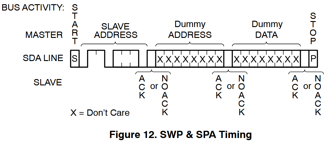
Aside from the page change commands, there’s some additional weirdness going on here. The SPAx commands also need two dummy bytes, which may or may not be ACKnowledged by the EEPROM.
I2C> [0b01101100 0x00 0x00]

I2C START
TX: 0b01101100 ACK
TX: 0x00 ACK 0x00 ACK
I2C STOP
I2C>
[- Start I2C transaction0b01101100- Send the SPA0 command to set page 00x00- Dummy byte 1, may be ACKnowledged0x00- Dummy byte 2, may be ACKnowledged]- End I2C transaction
Read page
I2C> [0xa0 0x00] [0xa1 r:256]

I2C START
TX: 0xA0 ACK 0x00 ACK
I2C STOP
I2C START
TX: 0xA1 ACK
RX: 0x23 ACK 0x11 ACK 0x0C ACK 0x03 ACK 0x84 ACK 0x19 ACK 0x00 ACK 0x08 ACK
    0x00 ACK 0x60 ACK 0x00 ACK 0x03 ACK 0x01 ACK 0x03 ACK 0x00 ACK 0x00 ACK
    0x00 ACK 0x00 ACK 0x07 ACK 0x0D ACK 0xF8 ACK 0x7F ACK 0x00 ACK 0x00 ACK
    0x6E ACK 0x6E ACK 0x6E ACK 0x11 ACK 0x00 ACK 0x6E ACK 0x20 ACK 0x08 ACK
    0x00 ACK 0x05 ACK 0x70 ACK 0x03 ACK 0x00 ACK 0xA8 ACK 0x1B ACK 0x28 ACK
    0x28 ACK 0x00 ACK 0x78 ACK 0x00 ACK 0x14 ACK 0x3C ACK 0x00 ACK 0x00 ACK
    0x00 ACK 0x00 ACK 0x00 ACK 0x00 ACK 0x00 ACK 0x00 ACK 0x00 ACK 0x00 ACK
    0x00 ACK 0x00 ACK 0x00 ACK 0x00 ACK 0x0C ACK 0x2B ACK 0x2D ACK 0x04 ACK
    0x16 ACK 0x35 ACK 0x23 ACK 0x0D ACK 0x00 ACK 0x00 ACK 0x2C ACK 0x0B ACK
    0x03 ACK 0x24 ACK 0x35 ACK 0x0C ACK 0x03 ACK 0x2D ACK 0x00 ACK 0x00 ACK
    0x00 ACK 0x00 ACK 0x00 ACK 0x00 ACK 0x00 ACK 0x00 ACK 0x00 ACK 0x00 ACK
    0x00 ACK 0x00 ACK 0x00 ACK 0x00 ACK 0x00 ACK 0x00 ACK 0x00 ACK 0x00 ACK
    0x00 ACK 0x00 ACK 0x00 ACK 0x00 ACK 0x00 ACK 0x00 ACK 0x00 ACK 0x00 ACK
    0x00 ACK 0x00 ACK 0x00 ACK 0x00 ACK 0x00 ACK 0x00 ACK 0x00 ACK 0x00 ACK
    0x00 ACK 0x00 ACK 0x00 ACK 0x00 ACK 0x00 ACK 0x00 ACK 0x9C ACK 0xB5 ACK
    0x00 ACK 0x00 ACK 0x00 ACK 0x00 ACK 0xE7 ACK 0xD6 ACK 0x34 ACK 0x9E ACK
    0x0F ACK 0x11 ACK 0x20 ACK 0x00 ACK 0x00 ACK 0x00 ACK 0x00 ACK 0x00 ACK
    0x00 ACK 0x00 ACK 0x00 ACK 0x00 ACK 0x00 ACK 0x00 ACK 0x00 ACK 0x00 ACK
    0x00 ACK 0x00 ACK 0x00 ACK 0x00 ACK 0x00 ACK 0x00 ACK 0x00 ACK 0x00 ACK
    0x00 ACK 0x00 ACK 0x00 ACK 0x00 ACK 0x00 ACK 0x00 ACK 0x00 ACK 0x00 ACK
    0x00 ACK 0x00 ACK 0x00 ACK 0x00 ACK 0x00 ACK 0x00 ACK 0x00 ACK 0x00 ACK
    0x00 ACK 0x00 ACK 0x00 ACK 0x00 ACK 0x00 ACK 0x00 ACK 0x00 ACK 0x00 ACK
    0x00 ACK 0x00 ACK 0x00 ACK 0x00 ACK 0x00 ACK 0x00 ACK 0x00 ACK 0x00 ACK
    0x00 ACK 0x00 ACK 0x00 ACK 0x00 ACK 0x00 ACK 0x00 ACK 0x00 ACK 0x00 ACK
    0x00 ACK 0x00 ACK 0x00 ACK 0x00 ACK 0x00 ACK 0x00 ACK 0x00 ACK 0x00 ACK
    0x00 ACK 0x00 ACK 0x00 ACK 0x00 ACK 0x00 ACK 0x00 ACK 0x00 ACK 0x00 ACK
    0x00 ACK 0x00 ACK 0x00 ACK 0x00 ACK 0x00 ACK 0x00 ACK 0x00 ACK 0x00 ACK
    0x00 ACK 0x00 ACK 0x00 ACK 0x00 ACK 0x00 ACK 0x00 ACK 0x00 ACK 0x00 ACK
    0x00 ACK 0x00 ACK 0x00 ACK 0x00 ACK 0x00 ACK 0x00 ACK 0x00 ACK 0x00 ACK
    0x00 ACK 0x00 ACK 0x00 ACK 0x00 ACK 0x00 ACK 0x00 ACK 0x00 ACK 0x00 ACK
    0x00 ACK 0x00 ACK 0x00 ACK 0x00 ACK 0x00 ACK 0x00 ACK 0x00 ACK 0x00 ACK
    0x00 ACK 0x00 ACK 0x00 ACK 0x00 ACK 0x00 ACK 0x00 ACK 0xEF ACK 0x55 NACK

I2C STOP
I2C>
Now that we’re on page 0, we can read the first 256 bytes of the SPD EEPROM. This requires two steps: first set the address to begin reading from, then read the data.
[0xa0 0x00]- Use the I2C write address (0xA0) to set the internal address pointer to 0x00.[ 0xa1 r:256 ]- Read 256 bytes from address 0x00 on page 0.
This reads the first 256 bytes of the SPD EEPROM. The data includes information about the module size, speed, timings, and other parameters.
Key Bytes
I2C> [0xa0 0x00] [0xa1 r:4]

I2C START
TX: 0xA0 ACK 0x00 ACK
I2C STOP
I2C START
TX: 0xA1 ACK
RX: 0x23 ACK 0x11 ACK 0x0C ACK 0x03 NACK
I2C STOP
I2C>
The first four bytes help us determine if this is a DDR4 module.
[0xa0 0x00]- Set the internal address pointer to 0.[0xa1 r:4]- Read the first four bytes of the SPD EEPROM.
The first four bytes are: 0x23 0x11 0x0C 0x03
| SPD Byte(s) | Definition |
|---|---|
| 0 | EEPROM size and bytes used |
| 1 | SPD revision |
| 2 | DRAM interface type |
| 3 | Memory module interface type |
Byte 2 (0x0C) is the DRAM device type. 0x0C indicates DDR4 SDRAM.
Byte 1 (0x11) encodes the SPD version. The high four bits are the major revision, the low four bits are the minor revision. 0x11 is revision 1.1.
Byte 3 (0x03 = 0b0000’0011) is the module type. The lower four bits indicate the type of module, 0b0010 is UDIMM and 0b0011 is SODIMM. There’s a large list of module types in JEDEC JESD21-C Annex L, so be sure to check there if you’re working with something exotic.
| Bits 3:0 | Type |
|---|---|
| 0010 | UDIMM |
| 0011 | SODIMM |
The upper four bits of byte 3 are used to indicate hybrid module types, which we won’t cover here.
Byte 0 (0x23 = 0b0010’0011) encodes the EEPROM size and number of bytes used. 010 = 512 total bytes, 0011 = 384 bytes used.
| Bit 7 | Bits 6-4 (SPD Bytes Total) | Bits 3-0 (SPD Bytes Used) |
|---|---|---|
| Reserved (0) | 000 = Undefined | 0000 = Undefined |
| 001 = 256 | 0001 = 128 | |
| 010 = 512 | 0010 = 256 | |
| All others = Reserved | 0011 = 384 | |
| 0100 = 512 | ||
| All others = Reserved |
Some information suggests that bit 7 of byte 0 determines the memory range included in the CRC calculation. However, according to JEDEC JESD21-C Annex L, bit 7 is reserved and must be coded as 0.
After the key bytes there is information about the SDRAM chips on the module: capacity, organization, speed, timings, etc. See the JEDEC JESD21-C Annex L standard for all the juicy details.
Manufacturer Info
| Byte Number | Address | Function |
|---|---|---|
| 320-321 | 0x140 | Module Manufacturer JEDEC ID |
| 323-324 | 0x143-0x144 | Module Manufacturing Date |
| 325-328 | 0x145-0x148 | Module Serial Number |
| 329-348 | 0x149-0x15C | Module Part Number |
| 350-351 | 0x15E | DRAM Manufacturer JEDEC ID |
| 353-381 | 0x161-0x17D | Module Manufacturer’s Specific Data |
| 382-383 | 0x17E-0x17F | Reserved |
This is a simplified table of the manufacturer information stored in the SPD EEPROM. Only the most interesting fields are shown here.
The manufacturer information is stored in page 1 of the EEPROM. Be sure to change to page 1 in the next step.
Module Manufacturer JEDEC ID
I2C> [0b01101110 0x00 0x00]

I2C START
TX: 0b01101110 ACK
TX: 0x00 ACK 0x00 ACK
I2C STOP
I2C> [0xa0 0x40] [0xa1 r:2]

I2C START
TX: 0xA0 ACK 0x40 ACK
I2C STOP
I2C START
TX: 0xA1 ACK
RX: 0x01 ACK 0x98 NACK
I2C STOP
I2C>
First we need to change to page 1 of the SPD EEPROM, then we can read the module manufacturer info.
[0b01101110 0x00 0x00]- Change to page 1 using the SPA1 command with two dummy bytes.
Because we’re reading from page 1, we need to subtract 256 (0x100) from the register addresses in the JEDEC standard. The module manufacturer JEDEC ID is stored in registers 320 and 321 (0x140, 0x141), which becomes 64 and 65 (0x40, 0x41) on page 1.
[0xa0 0x40] [0xa1 r:2]- Read the module manufacturer JEDEC ID.
0x01 is the least significant byte of JEDEC ID which determines which “bank” of the JEP106 list of IDs to search. 0x98 is the most significant byte, which is the actual manufacturer code. 0x9801 = Kingston Technology.
Module Manufacture Date
I2C> [0xa0 0x43] [0xa1 r:2]

I2C START
TX: 0xA0 ACK 0x43 ACK
I2C STOP
I2C START
TX: 0xA1 ACK
RX: 0x18 ACK 0x38 NACK
I2C STOP
I2C>
Read the module manufacturing date from registers 0x143-0x144, again subtract 256 bytes (0x43-0x44) to adjust for the page 1 address range. The date is encoded as a year and week number.
[0xa0 0x43][0xa1 r:2]- Read the module manufacturing date from address 0x43.
0x18 is the year, 0x38 is the week number. This module was manufactured in the 38th week of 2018.
Things not looking right? Be sure you change to page 1 before reading the manufacturer information.
Module Serial Number
I2C> [0xa0 0x45] [0xa1 r:4]

I2C START
TX: 0xA0 ACK 0x45 ACK
I2C STOP
I2C START
TX: 0xA1 ACK
RX: 0x84 ACK 0x24 ACK 0xA0 ACK 0x92 NACK
I2C STOP
I2C>
Read the module’s 4 byte serial number from registers 0x145-0x148 (page 1 address 0x45-0x46).
[0xa0 0x45][ 0xa1 r:4 ]- Read the module serial number.
0x84 0x24 0xA0 0x92 is the unique serial number.
The standard suggests using the full first 9 bytes (320-328) of manufacturing info (including the serial number) as the unique identifier for the module. The four byte unique serial number may not match anything printed on the module label.
Module Part Number
I2C> o

Number display format
 Current setting: Auto
 1. Auto
 2. HEX
 3. DEC
 4. BIN
 5. ASCII
 x. Exit
Mode > 5
Mode: ASCII
I2C>
The part number is a string of ASCII characters, so we’ll change the Bus Pirate output format to ASCII (type o, choose ASCII).
I2C> [0xa0 0x49] [0xa1 r:20]

I2C START
TX: 0xA0 ACK 0x49 ACK
I2C STOP
I2C START
TX: 0xA1 ACK
RX: 'A' 0x41 ACK 'C' 0x43 ACK 'R' 0x52 ACK '2' 0x32 ACK
    '4' 0x34 ACK 'D' 0x44 ACK '4' 0x34 ACK 'S' 0x53 ACK
    '7' 0x37 ACK 'S' 0x53 ACK '8' 0x38 ACK 'M' 0x4D ACK
    'B' 0x42 ACK '-' 0x2D ACK '4' 0x34 ACK ' ' 0x20 ACK
    ' ' 0x20 ACK ' ' 0x20 ACK ' ' 0x20 ACK ' ' 0x20 NACK

I2C STOP
I2C>
The part number is a 20 character ASCII text string starting at byte 329 (0x149). Remember to adjust the start address for page 1 (0x49).
[0xa0 0x49][ 0xa1 r:20 ]- Read the module part number.
The part number string is “ACR24D4S7S8MB-4”.
I2C> o

Number display format
 Current setting: ASCII
 1. Auto
 2. HEX
 3. DEC
 4. BIN
 5. ASCII
 x. Exit
Mode > 1
Mode: Auto
I2C>
Change the Bus Pirate output format back to AUTO before continuing (type o, choose AUTO).
DRAM Manufacturer JEDEC ID
I2C> [0xa0 0x5e][0xa1 r:2]

I2C START
TX: 0xA0 ACK 0x5E ACK
I2C STOP
I2C START
TX: 0xA1 ACK
RX: 0x80 ACK 0x2C NACK
I2C STOP
I2C>
There is a second JEDEC ID specifically to encode the DRAM chip manufacturer. We can grab this from bytes 350 and 351 (0x15E, 0x15F).
[0xa0 0x5e][0xa1 r:2]- Read the DRAM manufacturer JEDEC ID.
0x802C is the JEDEC ID for Micron Technology.
Manufacturer Specific Data
I2C> [0xa0 0x61][0xa1 r:29]

I2C START
TX: 0xA0 ACK 0x61 ACK
I2C STOP
I2C START
TX: 0xA1 ACK
RX: 0x00 ACK 0x00 ACK 0x00 ACK 0x00 ACK 0x00 ACK 0x00 ACK 0x00 ACK 0x00 ACK
    0x00 ACK 0x00 ACK 0x00 ACK 0x00 ACK 0x00 ACK 0x00 ACK 0x88 ACK 0x07 ACK
    0x38 ACK 0x31 ACK 0x35 ACK 0x33 ACK 0x31 ACK 0x37 ACK 0x33 ACK 0x00 ACK
    0x00 ACK 0x01 ACK 0x01 ACK 0x00 ACK 0x00 NACK
I2C STOP
I2C>
The last section (0x161-0x17D) is manufacturer specific data. This is a free area that can be used for anything the manufacturer wants, so it varies widely between manufacturers. It may contain additional overclocking profiles in EXPO (AMD) or XMP (Intel) format, it may also contain special keys that unscrupulous manufacturers use to lock a system to their specific brand of RAM module.
[0xa0 0x61][0xa1 r:29]- Read the manufacturer specific data from bytes 353 to 381 (0x161-0x17D).
This module has a bit of extra data, some binary and some ASCII encoded. The short ASCII string “8153173” appears, which matches a number printed on the module label.
EEPROM Block Protection
| Block | Byte Address Range | Hex Range | SPD Page Address |
|---|---|---|---|
| 0 | 0-127 | 0x00-0x7F | 0 |
| 1 | 128-255 | 0x80-0xFF | 0 |
| 2 | 256-383 | 0x100-0x17F | 1 |
| 3 | 384-511 | 0x180-0x1FF | 1 |
A software controlled write protection mechanism is available to prevent modification of the SPD EEPROM. Each 256 byte page has two 128 byte protection blocks.
Address pin SA0 must be connected to 9 volts to change the write protection settings. You can manually connect SA0 to 9 volts, or use an optocoupler to switch it under software control from the Bus Pirate IO2 pin. The DDR4 adapter plank has an optocoupler built in for this purpose, and a pin header to connect a 9 volt power supply (usually a 9 volt battery).
Check status
| Function | Abbr | b7 | b6 | b5 | b4 | b3 | b2 | b1 | b0 |
|---|---|---|---|---|---|---|---|---|---|
| Read Protection Status, block 0 | RPS0 | 0 | 1 | 1 | 0 | 0 | 0 | 1 | 1 |
| Read Protection Status, block 1 | RPS1 | 0 | 1 | 1 | 0 | 1 | 0 | 0 | 1 |
| Read Protection Status, block 2 | RPS2 | 0 | 1 | 1 | 0 | 1 | 0 | 1 | 1 |
| Read Protection Status, block 3 | RPS3 | 0 | 1 | 1 | 0 | 0 | 0 | 0 | 1 |
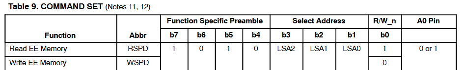
Four of those weird global commands test the protected status of each block.
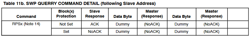
If protection is disabled the EEPROM responds with an ACK (0). If protection is enabled the EEPROM responds with a NACK (1). Again, these weird global commands need to be followed by two dummy bytes.
I2C> [0b01100011 0x00 0x00][0b01101001 0x00 0x00][0b01101011 0x00 0x00][0b01100001 0x00 0x00]

I2C START
TX: 0b01100011 NACK
TX: 0x00 NACK 0x00 NACK
I2C STOP
I2C START
TX: 0b01101001 NACK
TX: 0x00 NACK 0x00 NACK
I2C STOP
I2C START
TX: 0b01101011 ACK
TX: 0x00 NACK 0x00 NACK
I2C STOP
I2C START
TX: 0b01100001 ACK
TX: 0x00 NACK 0x00 NACK
I2C STOP
I2C>
[0b01100011 0x00 0x00]- Check the protection status of block 0 using the RPS0 command with two dummy bytes.[0b01101001 0x00 0x00]- Check the protection status of block 1 using the RPS1 command with two dummy bytes.[0b01101011 0x00 0x00]- Check the protection status of block 2 using the RPS2 command with two dummy bytes.[0b01100001 0x00 0x00]- Check the protection status of block 3 using the RPS3 command with two dummy bytes.
The first two blocks respons with NACK (1), indicating they are write protected. The last two blocks respond with ACK (0), indicating they are not write protected. This is the default configuration for most DDR4 modules.
Clear Protection
| Function | Abbr | b7 | b6 | b5 | b4 | b3 | b2 | b1 | b0 | A0 Pin |
|---|---|---|---|---|---|---|---|---|---|---|
| Clear All Write Protection | CWP | 0 | 1 | 1 | 0 | 0 | 1 | 1 | 0 | VHV |
A single command unlocks all blocks for writing. While this command is being sent, the SA0 pin must be connected to 9 volts (VHV) or the command will be ignored.
I2C> A 2
IO2 set to OUTPUT: 1

I2C> [0b01100110 0x00 0x00]

I2C START
TX: 0b01100110 ACK
TX: 0x00 ACK 0x00 ACK
I2C STOP
I2C> a 2
IO2 set to OUTPUT: 0

I2C>
First we enable the 9 volt supply to SA0, then we send the CWP command to clear all write protection. Again, this global command needs to be followed by two dummy bytes.
A 2- Connect SA0 to 9 volts using the optocoupler on IO2 pin (if using the DDR4 adapter plank).[0b01100110 0x00 0x00]- Clear all write protection using the CWP command with two dummy bytes.a 2- Disconnect SA0 from 9 volts, returning it to ground
I2C> [0b01100011 0x00 0x00]

I2C START
TX: 0b01100011 ACK
TX: 0x00 NACK 0x00 NACK
I2C STOP
I2C>
We can verify that all blocks are now unprotected by re-sending the protection status commands from earlier, the device should respond with ACK (0) for all blocks.
[0b01100011 0x00 0x00]- Check the protection status of block 0 using the RPS0 command with two dummy bytes.
Lock, unlock and writing data take time. While the operation is in progress, the SPD EEPROM will NACK all commands. This can be used to poll for completion by repeatedly sending a command until an ACK is received. NOTE: If SA0 is still connected to 9 volts when polling, the EEPROM address will change from 0x50 to 0x51. Adjust your polling commands accordingly or disable the 9 volt supply prior to polling the default address.
Set Protection
| Function | Abbr | b7 | b6 | b5 | b4 | b3 | b2 | b1 | b0 | A0 Pin |
|---|---|---|---|---|---|---|---|---|---|---|
| Set Write Protection, block 0 | SWP0 | 0 | 1 | 1 | 0 | 0 | 0 | 1 | 0 | VHV |
| Set Write Protection, block 1 | SWP1 | 0 | 1 | 1 | 0 | 1 | 0 | 0 | 0 | VHV |
| Set Write Protection, block 2 | SWP2 | 0 | 1 | 1 | 0 | 1 | 0 | 1 | 0 | VHV |
| Set Write Protection, block 3 | SWP3 | 0 | 1 | 1 | 0 | 0 | 0 | 0 | 0 | VHV |
While clearing write protection is all or nothing, setting write protection can be done one block at a time. Again, SA0 must be connected to 9 volts (VHV) while sending these commands.
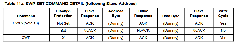
If protection is successfull, the EEPROM responds with ACK. Once again these global commands need to be followed by two dummy bytes.
I2C> A 2
IO2 set to OUTPUT: 1

I2C> [0b01100010 0x00 0x00]

I2C START
TX: 0b01100010 ACK
TX: 0x00 ACK 0x00 ACK
I2C STOP
I2C> [0b01101000 0x00 0x00]

I2C START
TX: 0b01101000 ACK
TX: 0x00 ACK 0x00 ACK
I2C STOP
I2C> a 2
IO2 set to OUTPUT: 0

I2C>
Enable the 9 volt supply to SA0, then set write protection for blocks 0 and 1.
A 2- Connect SA0 to 9 volts using the optocoupler on IO2 pin (if using the DDR4 adapter plank).[0b01100010 0x00 0x00]- Set write protection for block 0 using the SWP0 command with two dummy bytes.[0b01101000 0x00 0x00]- Set write protection for block 1 using the SWP1 command with two dummy bytes.a 2- Disconnect SA0 from 9 volts, returning it to ground
To verify, re-send the protection status commands from earlier. The device should respond with NACK (1) for blocks 0 and 1.
Write SPD EEPROM
Writing to the SPD EEPROM is dangerous!
- It can make the module unbootable.
- It can make the module unusable.
Before writing to the SPD EEPROM, make sure you have a backup of the original data. Better yet, only experiment with a module you don’t care about.
We’re going to write a 16 byte row in the End User Programmable area in page 1, 0x180-0x1FF. Despite the name, manufacturers do use this area to store overclocking profiles and other data. It is NOT safe to write in this area.
Read 16 Bytes
Writing to the SPD EEPROM is dangerous!
Before writing to the EEPROM, make sure you have a backup of the original data. Better yet, only experiment with a module you don’t care about.
In this step we will verify that the 16 byte row is empty before writing. If you see anything other than 0x00s ABSOLUTLY DO NOT WRITE TO THAT LOCATION. That area is already programmed with some data, and writing to it will make the module unbootable or unusable.
I2C> [0b01101110 0x00 0x00]

I2C START
TX: 0b01101110 ACK
TX: 0x00 ACK 0x00 ACK
I2C STOP
I2C> [0xa0 0xf0]

I2C START
TX: 0xA0 ACK 0xF0 ACK
I2C STOP
I2C> [0xa1 r:16]

I2C START
TX: 0xA1 ACK
RX: 0x00 ACK 0x00 ACK 0x00 ACK 0x00 ACK 0x00 ACK 0x00 ACK 0x00 ACK 0x00 ACK
    0x00 ACK 0x00 ACK 0x00 ACK 0x00 ACK 0x00 ACK 0x00 ACK 0x00 ACK 0x00 NACK

I2C STOP
I2C>
First let’s read the target row and make sure it’s empty. We’ll read 16 bytes from the last row of the EEPROM at address 0x1F0. Remember to subtract 0x100 to get the address relative to page 1 (0xF0).
[0b01101110 0x00 0x00]- Change to page 1 using the SPA1 command with two dummy bytes.[0xa0 0xf0]- Set the internal address pointer to 0xF0.[0xa1 r:16]- Read 16 bytes from address 0xF0 on page 1.
Every byte should be 0x00 if the row is empty.
If you see anything other than 0x00s, then ABSOLUTELY DO NOT WRITE TO THAT LOCATION. It is likely that area is already programmed with some data, and writing to it will make the module unbootable or unusable.
Write 16 Bytes
I2C> [0xa0 0xf0 1 2 3 4 5 6 7 8 9 10 11 12 13 14 15 16]

I2C START
TX: 0xA0 ACK 0xF0 ACK
TX: 1 ACK 2 ACK 3 ACK 4 ACK 5 ACK 6 ACK 7 ACK 8 ACK
    9 ACK 10 ACK 11 ACK 12 ACK 13 ACK 14 ACK 15 ACK 16 ACK

I2C STOP
I2C>
We can write from 1 to 16 bytes at a time, but there’s a rule. Writes are page aligned: the memory is divided into 16 byte pages (not to be confused with address pages 0/1), and writes cannot cross a page boundary. For example, if we start writing at address 0x1F0, we can write up to 16 bytes (0x1F0 to 0x1FF). If we start writing at address 0x1F5, we can only write 11 bytes (0x1F5 to 0x1FF), then the pointer rolls over back to the beginning of the page (0x1F0).
[0xa0 0xf0 1 2 3 4 5 6 7 8 9 10 11 12 13 14 15 16]- Write 16 bytes.
If you were writing a script or program to automate this, you would need to poll the device address until it responds with ACK indicating the write is complete. We’re moving slow enough that the write is complete by the next step.
Verify 16 Bytes
I2C> [0xa0 0xf0]

I2C START
TX: 0xA0 ACK 0xF0 ACK
I2C STOP
I2C> [0xa1 r:16]

I2C START
TX: 0xA1 ACK
RX: 0x01 ACK 0x02 ACK 0x03 ACK 0x04 ACK 0x05 ACK 0x06 ACK 0x07 ACK 0x08 ACK
    0x09 ACK 0x0A ACK 0x0B ACK 0x0C ACK 0x0D ACK 0x0E ACK 0x0F ACK 0x10 NACK

I2C STOP
I2C>
Finally! Let’s read back the 16 byte row to verify it was written correctly.
[0xa0 0xf0]- Set the internal address pointer to 0xF0.[0xa1 r:16]- Read the 16 byte row.
The read data should match the data we wrote: 1 2 3 4 5 6 7 8 9 10 11 12 13 14 15 16.
ddr4 Command
All of this demo and more is automated by the ddr4 command. It can read, write, verify, dump, lock and unlock the SPD hub non-volatile memory, decode the registers and even read the temperature sensor. Learn about the ddr4 command in the command reference.
Get a Bus Pirate
Get Bus Pirate & Accessories
- Browse Complete Bus Pirate hardware collection
- Bus Pirate 5 REV10 with enclosure
- Probe Cable Kit
- Auxiliary Cable Kit
- Quick Connect Adapter